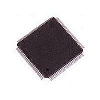
TDA8754HL11BE-S NXP Semiconductors, TDA8754HL11BE-S Datasheet - Page 16

TDA8754HL11BE-S
Manufacturer Part Number
TDA8754HL11BE-S
Description
Video ICs TRPL 8BIT VIDEO ADC
Manufacturer
NXP Semiconductors
Datasheet
1.TDA8754HL11C155.pdf
(57 pages)
Specifications of TDA8754HL11BE-S
Operating Supply Voltage
3 V to 3.6 V
Supply Current
180 mA
Maximum Operating Temperature
+ 70 C
Package / Case
SOT-486
Available Set Gain
6 dB
Bandwidth
700 MHz
Conversion Rate
110 msps
Maximum Power Dissipation
1.3 W
Minimum Operating Temperature
0 C
Mounting Style
SMD/SMT
Number Of Channels
3
Resolution
8 bit
Snr
48 dB
Lead Free Status / RoHS Status
Lead free / RoHS Compliant
Other names
TDA8754HL/11/C1,55
Philips Semiconductors
9397 750 14984
Product data sheet
8.4 PLL
8.5 Sync-on-green
Bit SCHCKREFO is used if in demultiplexed mode one pixel shift is needed in the DEO
signal (to move the screen one vertical line). By setting bit SCHCKREFO from a logic 0 to
a logic 1 a left move is obtained, also the timing relationship between HSYNCO, DEO and
CKDATA stays unchanged. An even number of pixel moves is done by changing the value
of HBACKL and HSYNCL. The correct combination of bits HBACKL, HSYNCL and
SCHCKREFO places the first active pixel at the beginning of the screen with always the
correct phase relationship between outputs DEO, HSYNCO and CKDATA.
Bit HSOSEL should be set to a logic 0 only after the PLL is stable, so only after the video
standard has been found and correct PLL parameters have been set in the TDA8754. Bit
HSOSEL should be set to a logic 1 to have a stable HSYNCO signal during the video
recognition. The video standard can be recognized by using the signals FIELDO,
VSYNCO and HSYNCO. The phase relation between CKDATA and HSYNCO (or DEO) is
undefined if bit HSOSEL = 1.
The ADCs are clocked by either the internal PLL locked to the reference clock (Hsync
from input or Hsync from sync separator) or to an external clock connected to pin CKEXT.
This selection is performed via the I
clock, bit CKEXT must be reset to logic 1.
The PLL phase frequency detector can be disconnected during the frame flyback (vertical
blanking) or the unavailability of the Ckref signal by using the coast function. The coast
signal can be derived from the VSYNC1(2) input, from the Vsync extracted by the sync
separator or from the coast input. The coast function can be disabled with bit COE.
The coast signal may be active either HIGH or LOW by setting bit COS.
It is possible to control the phase of the ADC clock via the I
phase-shift controller. The phase register (5 bits) enables to shift the phase by steps of
11.25 deg.
The PLL also provides a CKDATA clock. This clock is synchronized with the data outputs
whatever the output mode is.
It is possible to delay the CKDATA clock with a constant delay (t = 2 ns compared to the
outputs) by setting bit CKDD = 1. Moreover, it is possible to invert this output by setting
bit CKDATINV = 1.
When the PLL reference signal comes from the separator, the PLL rising edge must be
preferably used in order to not use the PLL coast mode. It should be noted that the
HSYNCO output of the sync separator is always a mostly low signal, whatever is the
polarity of the composite sync input. The VSYNCO output signal of the sync separator is
also mostly low signal. It is at a high state during the vertical blanking.
When the SOG input is selected (bit SOGSEL = 1), the SOG charge pump current bits
SOGI[1:0] should be programmed in function of the input signal; see
A hum remover is implemented in the SOG. It removes completely the hum perturbation
on the first or second edge of the horizontal sync pulse for digital video input like VESA,
and on the second edge only for analog video input signal like TV or HDTV.
Rev. 06 — 16 June 2005
2
C-bus by setting bit CKEXT. To use the external
Triple 8-bit video ADC up to 270 Msps
2
© Koninklijke Philips Electronics N.V. 2005. All rights reserved.
C-bus with the included digital
Table
TDA8754
5.
16 of 57


