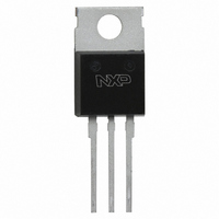
BUK7528-55A,127 NXP Semiconductors, BUK7528-55A,127 Datasheet

BUK7528-55A,127
Specifications of BUK7528-55A,127
BUK7528-55A
BUK7528-55A
Related parts for BUK7528-55A,127
BUK7528-55A,127 Summary of contents
Page 1
... DS(ON) resistance V GS PIN CONFIGURATION tab SOT404 TO220AB BUK7528-55A BUK7628-55A CONDITIONS - ˚ 100 ˚ ˚ ˚ CONDITIONS - in free air Minimum footprint, FR4 board 1 Product specification BUK7528-55A BUK7628-55A MAX. UNIT 175 = SYMBOL MIN. MAX. UNIT - 168 - 175 TYP. MAX. UNIT - 1.5 K K/W ...
Page 2
... Measured from drain lead 6 mm from package to centre of die Measured from contact screw on tab to centre of die(TO220AB) Measured from upper edge of drain tab to centre of die(SOT404) Measured from source lead to source bond pad CONDITIONS -dI /dt = 100 - Product specification BUK7528-55A BUK7628-55A MIN. TYP. MAX. UNIT 4 0. ...
Page 3
... CONDITIONS 1000 100 10 1 120 140 160 180 = f 0.1 0.01 0.000001 120 140 160 180 Product specification BUK7528-55A BUK7628-55A MIN. TYP ˚ RDS(on) = VDS 10us 100 D. 100 100 VDS / V Fig.3. Safe operating area & f single pulse; parameter Zth / (K/ 0.5 0.2 0 0.05 ...
Page 4
... 8 9 ˚C. Fig.9. Typical transconductance 2.5 1.5 0 ˚C. Fig.10. Normalised drain-source on-state resistance Product specification BUK7528-55A BUK7628-55A ˚C = 175 VGS/V Fig.8. Typical transfer characteristics conditions parameter gfs / f(I ); conditions Rds(on) normlised to 25degC 2 1 -100 - 100 Tmb / degC / DS(ON) DS(ON)25 ˚ ...
Page 5
... Ciss Coss 100 Fig.16. Normalised avalanche energy rating. iss oss rss = MHz 5 Product specification BUK7528-55A BUK7628-55A VGS / V VDS= 14V VDS= 44V f(Q ); conditions parameter 175 Tj / ˚ 0.0 0.5 VSDS / V 1.0 Fig.15. Typical reverse diode current. = f(V ); conditions parameter T ...
Page 6
... Philips Semiconductors TrenchMOS transistor Standard level FET L VGS 0 RGS Fig.17. Avalanche energy test circuit 0 DSS D DSS June 2000 VDD + VDS - VGS -ID/100 T.U. shunt BV V DSS DD 6 Product specification BUK7528-55A BUK7628-55A + RD VDS - RG T.U.T. Fig.18. Switching test circuit. VDD Rev 1.100 ...
Page 7
... Note 1. Terminals in this zone are not tinned. REFERENCES OUTLINE VERSION IEC JEDEC SOT78 TO-220 Fig.19. SOT78 (TO220AB); pin 2 connected to mounting base. 7 Product specification BUK7528-55A BUK7628-55A scale ( max. 10.3 15.0 3.30 3 ...
Page 8
... Epoxy meets UL94 V0 at 1/8". June 2000 2 scale max. 0.85 0.64 1.60 10.30 2.90 15.40 11 2.54 0.60 0.46 1.20 9.70 2.10 14.80 REFERENCES IEC JEDEC EIAJ 8 Product specification BUK7528-55A BUK7628-55A 2 -PAK); 3 leads SOT404 mounting base 2.60 2.20 EUROPEAN ISSUE DATE PROJECTION 98-12-14 99-06-25 Rev 1.100 ...
Page 9
... Philips for any damages resulting from such improper use or sale. June 2000 11.5 9.0 2.0 3.8 5.08 Fig.21. SOT404 : soldering pattern for surface mounting. 9 Product specification BUK7528-55A BUK7628-55A 17.5 Rev 1.100 ...


