BUK9609-75A,118 NXP Semiconductors, BUK9609-75A,118 Datasheet
BUK9609-75A,118
Specifications of BUK9609-75A,118
BUK9609-75A /T3
BUK9609-75A /T3


Related parts for BUK9609-75A,118


BUK9609-75A,118 Summary of contents
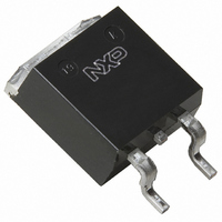
Page 1
... BUK9609-75A N-channel TrenchMOS logic level FET Rev. 03 — 22 September 2008 1. Product profile 1.1 General description Logic level N-channel enhancement mode Field-Effect Transistor (FET plastic package using TrenchMOS technology. This product has been designed and qualified to the appropriate AEC standard for use in automotive critical applications. ...
Page 2
... ° °C; see Figure 2 mb ≤ 50 µs pulsed °C mb ≤ 10 µs; pulsed ° ≤ Ω sup °C; unclamped j(init) Rev. 03 — 22 September 2008 BUK9609-75A N-channel TrenchMOS logic level FET Graphic symbol mbb076 Version SOT404 Min Max - - Figure Figure 3 - 440 - 230 ...
Page 3
... T (°C) mb Fig 2. Normalized total power dissipation as a function of mounting base temperature R DSon = D. δ Rev. 03 — 22 September 2008 BUK9609-75A N-channel TrenchMOS logic level FET 03na19 50 100 150 200 T (°C) mb 03nb44 100 100 (V) 100 © NXP B.V. 2008. All rights reserved. ...
Page 4
... Fig 4. Transient thermal impedance from junction to mounting base as a function of pulse duration BUK9609-75A_3 Product data sheet Conditions see Figure 4 minimum footprint; mounted on a printed-circuit board Rev. 03 — 22 September 2008 BUK9609-75A N-channel TrenchMOS logic level FET Min Typ Max - - 0. 03nb45 t p δ ...
Page 5
... °C j from source lead to source bond pad ° °C; see Figure /dt = -100 A/µ - ° Rev. 03 — 22 September 2008 BUK9609-75A N-channel TrenchMOS logic level FET Min Typ Max 1 500 - 0. 100 - 2 ...
Page 6
... V (V) GS Fig 6. Gate-source threshold voltage as a function of junction temperature 03nb41 R DSon (mΩ 2 (V) Fig 8. Drain-source on-state resistance as a function of gate-source voltage; typical values Rev. 03 — 22 September 2008 BUK9609-75A N-channel TrenchMOS logic level FET 03aa33 max typ min 0 60 120 ( ° ...
Page 7
... I D (A) Fig 10. Transfer characteristics: drain current as a function of gate-source voltage; typical values 03nb37 R DSon (mΩ 100 150 Q G (nC) Fig 12. Drain-source on-state resistance as a function of drain current; typical values Rev. 03 — 22 September 2008 BUK9609-75A N-channel TrenchMOS logic level FET 175 0.0 1.0 2 ...
Page 8
... V SD (V) Fig 14. Input, output and reverse transfer capacitances as a function of drain-source voltage; typical values 2.4 a 1.6 0.8 0 − 120 Rev. 03 — 22 September 2008 BUK9609-75A N-channel TrenchMOS logic level FET 03nb43 0 0.01 0 (V) 03nb25 180 T (°C) j © NXP B.V. 2008. All rights reserved. ...
Page 9
... max. 1.60 10.30 2.90 15.80 11 2.54 1.20 9.70 2.10 14.80 REFERENCES JEDEC JEITA Rev. 03 — 22 September 2008 BUK9609-75A N-channel TrenchMOS logic level FET mounting base 2.60 2.20 EUROPEAN ISSUE DATE PROJECTION 05-02-11 06-03-16 © NXP B.V. 2008. All rights reserved. SOT404 ...
Page 10
... The format of this data sheet has been redesigned to comply with the new identity guidelines of NXP Semiconductors. • Legal texts have been adapted to the new company name where appropriate. • Type number BUK9609-75A separated from data sheet BUK9509_9609_75A-02. BUK9509_9609_75A-02 20001106 BUK9509_9609_75A-01 20001010 ...
Page 11
... Notice: All referenced brands, product names, service names and trademarks are the property of their respective owners. TrenchMOS — trademark of NXP B.V. http://www.nxp.com salesaddresses@nxp.com Rev. 03 — 22 September 2008 BUK9609-75A N-channel TrenchMOS logic level FET © NXP B.V. 2008. All rights reserved ...
Page 12
... Please be aware that important notices concerning this document and the product(s) described herein, have been included in section ‘Legal information’. © NXP B.V. 2008. For more information, please visit: http://www.nxp.com For sales office addresses, please send an email to: salesaddresses@nxp.com Date of release: Rev. 03 — 22 September 2008 Document identifier: BUK9609-75A_3 All rights reserved. ...