IRF7321D2TRPBF International Rectifier, IRF7321D2TRPBF Datasheet
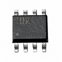
MOSFET P-CH 30V 4.7A 8-SOIC

IRF7321D2TRPBF

Manufacturer Part Number
IRF7321D2TRPBF
Description
MOSFET P-CH 30V 4.7A 8-SOIC
Manufacturer
International Rectifier
Series
FETKY™r
Datasheet

Specifications of IRF7321D2TRPBF

Fet Type
MOSFET P-Channel, Metal Oxide
Fet Feature
Diode (Isolated)
Rds On (max) @ Id, Vgs
62 mOhm @ 4.9A, 10V
Drain To Source Voltage (vdss)
30V
Current - Continuous Drain (id) @ 25° C
4.7A
Vgs(th) (max) @ Id
1V @ 250µA
Gate Charge (qg) @ Vgs
34nC @ 10V
Input Capacitance (ciss) @ Vds
710pF @ 25V
Power - Max
2W
Mounting Type
Surface Mount
Package / Case
8-SOIC (3.9mm Width)
Transistor Polarity
P-Channel
Resistance Drain-source Rds (on)
98 mOhms
Drain-source Breakdown Voltage
- 30 V
Gate-source Breakdown Voltage
20 V
Continuous Drain Current
- 4.9 A
Power Dissipation
2 W
Mounting Style
SMD/SMT
Gate Charge Qg
23 nC
Lead Free Status / RoHS Status
Lead free / RoHS Compliant
Other names
IRF7321D2PBFTR
Description
The FETKY
Schottky diodes offer the designer an innovative board
space saving solution for switching regulator
power management applications.
HEXFETs utilize advanced processing techniques to
achieve extremely low on-resistance per silicon area.
Combinining this technology with International
Rectifier's low forward drop Schottky rectifiers results in
an extremely efficient device suitable for use in a wide
variety of portable electronics applications.
The SO-8 has been modified through a customized
leadframe for enhanced thermal characteristics. The
SO-8 package is designed for vapor phase, infrared or
wave soldering techniques.
Absolute Maximum Ratings ( T
Thermal Resistance Ratings
Notes:

ƒ
l
l
l
l
l
l
l
R
I
I
I
P
P
V
dv/dt
T
D
D
DM
θJA
Pulse width ≤ 300µs – duty cycle ≤ 2%
D
D
GS
J,
Low V
Repetitive rating – pulse width limited by max. junction temperature (see fig. 11)
I
Surface mounted on FR-4 board, t ≤ 10sec.
Co-packaged HEXFET® Power
MOSFET and Schottky Diode
Ideal For Buck Regulator Applications
P-Channel HEXFET®
Generation 5 Technology
SO-8 Footprint
Lead-Free
@ T
@ T
SD
T
@T
@T
STG
≤ -2.9A, di/dt ≤ -77A/µs, V
A
A
A
A
= 25°C
= 70°C
= 25°C
= 70°C
F
TM
Schottky Rectifier
family of Co-packaged HEXFETs and
Parameter
Continuous Drain Current, V
Pulsed Drain Current À
Power Dissipation
Linear Derating Factor
Gate-to-Source Voltage
Peak Diode Recovery dv/dt Á
Junction and Storage Temperature Range
Parameter
Junction-to-Ambient
DD
≤ V
(BR)DSS
Generation 5
A
, T
= 25°C Unless Otherwise Noted)
J
≤ 150°C
Ã
and
GS
A
S
G
A
@ -10V
FETKY MOSFET & Schottky Diode
1
2
3
4
Top View
IRF7321D2PbF
8
7
6
5
-55 to +150
Maximum
SO-8
± 20
-4.7
-3.8
-5.0
Maximum
-38
K
2.0
1.3
K
D
D
16
62.5
Schottky Vf = 0.52V
R
DS(on)
V
DSS
www.irf.com
= 0.062Ω
PD - 95297
= -30V
Units
mW/°C
°C/W
Units
V/ns
°C
W
A
V

Related parts for IRF7321D2TRPBF

IRF7321D2TRPBF Summary of contents

Page 1

Co-packaged HEXFET® Power l MOSFET and Schottky Diode Ideal For Buck Regulator Applications l P-Channel HEXFET® l Low V Schottky Rectifier l F Generation 5 Technology l SO-8 Footprint l Lead-Free l Description TM The FETKY family of Co-packaged HEXFETs ...

Page 2

... Vfm Max. Forward voltage drop Irm Max. Reverse Leakage current Ct Max. Junction Capacitance dv/dt Max. Voltage Rate of Charge ( HEXFET is the reg. TM for International Rectifier Power MOSFET 25°C (unless otherwise specified) J Min. Typ. Max. Units Conditions -30 ––– ––– ...

Page 3

VGS TOP - 15V - 10V - 7.0V - 5.5V - 4.5V - 4.0V - 3.5V BOTTOM - 3.0V 10 20µs PULSE WIDTH T = 25° 0 Drain-to-Source Voltage (V) DS 100 T = ...

Page 4

Power Mosfet Characteristics 1400 GS 1200 1000 C iss 800 C oss 600 400 C rss 200 Drain-to-Source Voltage (V) DS Fig 5. Typical Capacitance Vs. Drain-to-Source Voltage 100 T = 150° ...

Page 5

SINGLE PULSE (THERMAL RESPONSE) 0.1 0.00001 0.0001 0.001 0.6 0.5 0.4 0 -4.5V GS 0.2 0.1 0 www.irf.com Power Mosfet Characteristics 0.01 0 Rectangular Pulse ...

Page 6

Schottky Diode Characteristics 100 150° 125° 25°C 1 0.1 0.0 0.2 0.4 0.6 Forward Voltage Drop - V Forward Voltage Drop - V Fig Typical Forward Voltage Drop Characteristics 6 1 ...

Page 7

SO-8 (Fetky) Package Outline 0.25 [.010 NOT DIMENS IONING & T OLERANCING PER AS ME Y14.5M-1994. ...

Page 8

SO-8 Tape and Reel Dimensions are shown in milimeters (inches) This product has been designed and qualified for the Consumer market. IR WORLD HEADQUARTERS: 233 Kansas St., El Segundo, California 90245, USA Tel: (310) 252-7105 8 TERMINAL NUMBER 1 8.1 ...

Related keywords