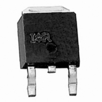
IRFR3711PBF International Rectifier, IRFR3711PBF Datasheet - Page 2
IRFR3711PBF
Manufacturer Part Number
IRFR3711PBF
Description
MOSFET N-CH 20V 100A DPAK
Manufacturer
International Rectifier
Series
HEXFET®r
Datasheet
1.IRFU3711PBF.pdf
(11 pages)
Specifications of IRFR3711PBF
Fet Type
MOSFET N-Channel, Metal Oxide
Fet Feature
Logic Level Gate
Rds On (max) @ Id, Vgs
6.5 mOhm @ 15A, 10V
Drain To Source Voltage (vdss)
20V
Current - Continuous Drain (id) @ 25° C
100A
Vgs(th) (max) @ Id
3V @ 250µA
Gate Charge (qg) @ Vgs
44nC @ 4.5V
Input Capacitance (ciss) @ Vds
2980pF @ 10V
Power - Max
2.5W
Mounting Type
Surface Mount
Package / Case
DPak, TO-252 (2 leads+tab), SC-63
Transistor Polarity
N-Channel
Resistance Drain-source Rds (on)
8.5 mOhms
Drain-source Breakdown Voltage
20 V
Gate-source Breakdown Voltage
20 V
Continuous Drain Current
110 A
Power Dissipation
120 W
Mounting Style
SMD/SMT
Gate Charge Qg
29 nC
Lead Free Status / RoHS Status
Lead free / RoHS Compliant
Available stocks
Company
Part Number
Manufacturer
Quantity
Price
Company:

Part Number:
IRFR3711PBF
Manufacturer:
INTERNATIONAL RECTIFIER
Quantity:
30 000


∆V
Static @ T
V
R
V
I
I
Dynamic @ T
g
Q
Q
Q
Q
R
t
t
t
t
C
C
C
Avalanche Characteristics
E
I
Diode Characteristics
I
I
V
t
Q
t
Q
DSS
GSS
d(on)
r
d(off)
f
AR
S
SM
rr
rr
fs
(BR)DSS
DS(on)
GS(th)
G
iss
oss
rss
AS
SD
2
g
gs
gd
oss
rr
rr
(BR)DSS
Symbol
Symbol
Symbol
Symbol
/∆T
J
J
Drain-to-Source Breakdown Voltage
Breakdown Voltage Temp. Coefficient
Static Drain-to-Source On-Resistance
Gate Threshold Voltage
Drain-to-Source Leakage Current
Gate-to-Source Forward Leakage
Gate-to-Source Reverse Leakage
Forward Transconductance
Total Gate Charge
Gate-to-Source Charge
Gate-to-Drain ("Miller") Charge
Output Gate Charge
Gate Resistance
Turn-On Delay Time
Rise Time
Turn-Off Delay Time
Fall Time
Input Capacitance
Output Capacitance
Reverse Transfer Capacitance
Single Pulse Avalanche Energy
Avalanche Current
Continuous Source Current
(Body Diode)
Pulsed Source Current
(Body Diode)
Diode Forward Voltage
Reverse Recovery Time
Reverse Recovery Charge
Reverse Recovery Time
Reverse Recovery Charge
= 25°C (unless otherwise specified)
J
Parameter
= 25°C (unless otherwise specified)
Ù
Parameter
Parameter
Parameter
Ù
Min
Min
Min
–––
–––
–––
–––
–––
–––
–––
–––
–––
–––
–––
–––
–––
–––
–––
–––
–––
–––
–––
–––
–––
–––
–––
–––
–––
–––
–––
1.0
0.3
20
53
0.022
2980
1770
Typ
Typ
Typ
0.88
0.82
–––
–––
–––
–––
–––
–––
–––
–––
220
280
–––
–––
–––
5.2
6.7
7.3
8.9
29
33
12
17
12
50
61
48
65
110
Max Units
Max Units
Max Units
-200
Typ
–––
–––
140
100
200
–––
–––
–––
–––
–––
–––
–––
–––
–––
–––
–––
–––
–––
440
–––
6.5
8.5
3.0
2.5
1.3
20
44
75
92
72
98
f
V/°C
mΩ
µA
nA
nC
nC
nC
pF
ns
ns
ns
Ω
V
V
S
A
V
V
Reference to 25°C, I
V
V
V
V
V
V
V
V
V
I
V
V
V
V
I
R
V
V
V
ƒ = 1.0MHz
MOSFET symbol
showing the
integral reverse
p-n junction diode.
T
T
T
di/dt = 100A/µs
T
di/dt = 100A/µs
D
D
J
J
J
J
GS
GS
GS
DS
DS
DS
DS
GS
GS
DS
DS
GS
GS
DD
GS
GS
DS
G
= 15A
= 30A
= 25°C, I
= 125°C, I
= 25°C, I
= 125°C, I
= 1.8Ω
= V
= 20V, V
= 16V, V
= 16V, V
= 16V, I
= 10V
= 10V
= 0V, I
= 10V, I
= 4.5V, I
= 20V
= -20V
= 4.5V
= 0V, V
= 10V
= 4.5V
= 0V
GS
Max
460
, I
30
D
Conditions
Conditions
e
e
Conditions
D
DS
S
F
D
D
= 250µA
D
GS
GS
GS
S
F
= 250µA
= 16A, V
= 30A, V
= 30A
= 15A
= 10V
= 12A
= 16A, V
= 30A, V
= 0V
= 0V
= 0V, T
e
e
www.irf.com
D
e
e
= 1mA
R
GS
J
R
GS
= 10V
= 125°C
= 10V
= 0V
= 0V
Units
mJ
A
e
e
Related parts for IRFR3711PBF
Image
Part Number
Description
Manufacturer
Datasheet
Request
R

Part Number:
Description:
Power MOSFET(Vdss=100V, Rds(on)=0.21ohm, Id=9.4A)
Manufacturer:
IRF [International Rectifier]
Datasheet:
Part Number:
Description:
Advanced Power MOSFET
Manufacturer:
FAIRCHILD [Fairchild Semiconductor]
Datasheet:

Part Number:
Description:
SCHOTTKY RECTIFIER
Manufacturer:
International Rectifier Corp.
Datasheet:
Part Number:
Description:
SCHOTTKY RECTIFIER
Manufacturer:
International Rectifier Corp.
Datasheet:
Part Number:
Description:
SCHOTTKY RECTIFIER
Manufacturer:
International Rectifier Corp.
Datasheet:
Part Number:
Description:
SCHOTTKY RECTIFIER
Manufacturer:
International Rectifier Corp.
Datasheet:
Part Number:
Description:
SCHOTTKY RECTIFIER
Manufacturer:
International Rectifier Corp.
Datasheet:
Part Number:
Description:
SCHOTTKY RECTIFIER
Manufacturer:
International Rectifier Corp.
Datasheet:
Part Number:
Description:
SCHOTTKY RECTIFIER
Manufacturer:
International Rectifier Corp.
Datasheet:
Part Number:
Description:
SCHOTTKY RECTIFIER
Manufacturer:
International Rectifier Corp.
Datasheet:
Part Number:
Description:
SCHOTTKY RECTIFIER
Manufacturer:
International Rectifier Corp.
Datasheet:
Part Number:
Description:
SCHOTTKY RECTIFIER
Manufacturer:
International Rectifier Corp.
Datasheet:
Part Number:
Description:
SCHOTTKY RECTIFIER
Manufacturer:
International Rectifier Corp.
Datasheet:
Part Number:
Description:
SCHOTTKY RECTIFIER
Manufacturer:
International Rectifier Corp.
Datasheet:
Part Number:
Description:
SCHOTTKY RECTIFIER
Manufacturer:
International Rectifier Corp.
Datasheet: