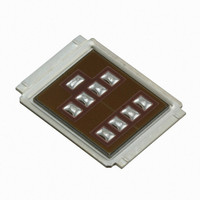
IRF7799L2TRPBF International Rectifier, IRF7799L2TRPBF Datasheet - Page 6

IRF7799L2TRPBF
Manufacturer Part Number
IRF7799L2TRPBF
Description
MOSFET N-CH 250V DIRECTFET L8
Manufacturer
International Rectifier
Series
HEXFET®r
Datasheet
1.IRF7799L2TRPBF.pdf
(11 pages)
Specifications of IRF7799L2TRPBF
Fet Type
MOSFET N-Channel, Metal Oxide
Fet Feature
Standard
Rds On (max) @ Id, Vgs
38 mOhm @ 21A, 10V
Drain To Source Voltage (vdss)
250V
Current - Continuous Drain (id) @ 25° C
375A
Vgs(th) (max) @ Id
5V @ 250µA
Gate Charge (qg) @ Vgs
165nC @ 10V
Input Capacitance (ciss) @ Vds
6714pF @ 25V
Power - Max
4.3W
Mounting Type
Surface Mount
Package / Case
DirectFET™ Isometric L8
Transistor Polarity
N-Channel
Drain-source Breakdown Voltage
250 V
Gate-source Breakdown Voltage
30 V
Continuous Drain Current
35 A
Power Dissipation
125 W
Gate Charge Qg
110 nC
Lead Free Status / RoHS Status
Lead free / RoHS Compliant
Available stocks
Company
Part Number
Manufacturer
Quantity
Price
Company:
Part Number:
IRF7799L2TRPBF
Manufacturer:
UCHIHASHI
Quantity:
10 000
Fig 16. Maximum Avalanche Energy Vs. Temperature
6
350
300
250
200
150
100
50
‚
100
0
0.1
+
-
10
1.0E-06
1
25
Starting T J , Junction Temperature (°C)
D.U.T
Allowed avalanche Current vs avalanche
pulsewidth, tav, assuming ∆Τ j = 25°C and
Tstart = 150°C.
Fig 17.
50
Duty Cycle = Single Pulse
ƒ
TOP
BOTTOM 1.0% Duty Cycle
I D = 21A
75
+
-
•
•
•
•
SD
0.10
0.05
0.01
1.0E-05
100
•
•
•
Fig 15. Typical Avalanche Current Vs.Pulsewidth
Single Pulse
125
-
G
„
150
+
1.0E-04
175
+
-
tav (sec)
Re-Applied
Voltage
Reverse
Recovery
Current
for N-Channel HEXFET
Driver Gate Drive
D.U.T. I
D.U.T. V
Inductor Curent
Allowed avalanche Current vs avalanche
pulsewidth, tav, assuming ∆Tj = 150°C and
Tstart =25°C (Single Pulse)
Notes on Repetitive Avalanche Curves , Figures 13, 14:
(For further info, see AN-1005 at www.irf.com)
1. Avalanche failures assumption:
2. Safe operation in Avalanche is allowed as long asT
3. Equation below based on circuit and waveforms shown in
4. P
5. BV = Rated breakdown voltage (1.3 factor accounts for
6. I
7. ∆T
1.0E-03
t
Z
Purely a thermal phenomenon and failure occurs at a
temperature far in excess of T
every part type.
not exceeded.
Figures 16a, 16b.
avalanche pulse.
voltage increase during avalanche).
T
D = Duty cycle in avalanche = t
av
av =
thJC
D (ave)
jmax
P.W.
SD
DS
= Allowable avalanche current.
=
Average time in avalanche.
(D, t
Waveform
Allowable rise in junction temperature, not to exceed
Waveform
(assumed as 25°C in Figure 15, 16).
= Average power dissipation per single
av
Ripple ≤ 5%
Body Diode
P
Period
) = Transient thermal resistance, see figure 11)
D (ave)
Body Diode Forward
Diode Recovery
Current
= 1/2 ( 1.3·BV·I
I
av
E
AS (AR)
1.0E-02
dv/dt
Forward Drop
= 2DT/ [1.3·BV·Z
®
di/dt
Power MOSFETs
= P
D =
jmax
D (ave)
av
av
Period
. This is validated for
P.W.
·f
) = DT/ Z
·t
th
a
]
1.0E-01
V
V
I
SD
thJC
GS
DD
www.irf.com
=10V
jmax
is


