IRLS3034-7PPBF International Rectifier, IRLS3034-7PPBF Datasheet

MOSFET N-CH 40V 240A D2PAK-7

IRLS3034-7PPBF

Manufacturer Part Number
IRLS3034-7PPBF
Description
MOSFET N-CH 40V 240A D2PAK-7
Manufacturer
International Rectifier
Series
HEXFET®r
Datasheet

Specifications of IRLS3034-7PPBF

Fet Type
MOSFET N-Channel, Metal Oxide
Fet Feature
Logic Level Gate
Rds On (max) @ Id, Vgs
1.4 mOhm @ 200A, 10V
Drain To Source Voltage (vdss)
40V
Current - Continuous Drain (id) @ 25° C
240A
Vgs(th) (max) @ Id
2.5V @ 250µA
Gate Charge (qg) @ Vgs
180nC @ 4.5V
Input Capacitance (ciss) @ Vds
10990pF @ 40V
Power - Max
380W
Mounting Type
Surface Mount
Package / Case
D²Pak, TO-263 (6 leads + tab)
Transistor Polarity
N-Channel
Resistance Drain-source Rds (on)
1.7 mOhms
Drain-source Breakdown Voltage
40 V
Gate-source Breakdown Voltage
20 V
Continuous Drain Current
380 A
Power Dissipation
380 W
Mounting Style
SMD/SMT
Gate Charge Qg
120 nC
Lead Free Status / RoHS Status
Lead free / RoHS Compliant

Available stocks

Company
Part Number
Manufacturer
Quantity
Price
Part Number:
IRLS3034-7PPBF
Manufacturer:
IR
Quantity:
9 140
Applications
l
l
l
l
l
www.irf.com
Benefits
l
l
l
l
l
l
l
Absolute Maximum Ratings
I
I
I
I
P
V
dv/dt
T
T
Avalanche Characteristics
E
I
E
Thermal Resistance
R
R
D
D
D
DM
AR
J
STG
D
GS
AS (Thermally limited)
AR
θJC
θJA
@ T
@ T
@ T
High Efficiency Synchronous Rectification in SMPS
DC Motor Drive
Uninterruptible Power Supply
High Speed Power Switching
Hard Switched and High Frequency Circuits
Optimized for Logic Level Drive
Very Low R
Superior R*Q at 4.5V V
Improved Gate, Avalanche and Dynamic dV/dt
Ruggedness
Fully Characterized Capacitance and Avalanche
Enhanced body diode dV/dt and dI/dt Capability
Lead-Free
@T
SOA
Symbol
Symbol
C
C
C
C
= 25°C
= 100°C
= 25°C
= 25°C
DS(ON)
Continuous Drain Current, V
Pulsed Drain Current d
Maximum Power Dissipation
Linear Derating Factor
Gate-to-Source Voltage
Peak Diode Recovery f
Operating Junction and
Storage Temperature Range
Soldering Temperature, for 10 seconds
(1.6mm from case)
Single Pulse Avalanche Energy e
Avalanche Current d
Repetitive Avalanche Energy d
Junction-to-Case kl
Junction-to-Ambient j
at 4.5V V
GS
GS
Parameter
Parameter
GS
GS
GS
@ 10V (Silicon Limited)
@ 10V (Wire Bond Limited)
G
Gate
IRLS3034-7PPbF
G
D
S
See Fig. 14, 15, 22a, 22b
Typ.
–––
–––
V
R
I
I
D
D
D
DSS
DS(on)
(Silicon Limited)
(Package Limited)
-55 to + 175
Drain
Max.
380c
270c
HEXFET
1540
240
380
± 20
300
250
2.5
1.3
D
G
typ.
S
max.
S
S
Max.
0.40
S
®
40
S
Power MOSFET
Source
380A c
1.0m Ω
1.4m Ω
240A
S
40V
Units
Units
W/°C
°C/W
V/ns
mJ
mJ
°C
W
A
V
A
1/12/09
1

Related parts for IRLS3034-7PPBF

IRLS3034-7PPBF Summary of contents

Page 1

... Avalanche Characteristics Single Pulse Avalanche Energy (Thermally limited) Avalanche Current Repetitive Avalanche Energy Thermal Resistance Symbol R Junction-to-Case kl θJC R Junction-to-Ambient j θJA www.irf.com IRLS3034-7PPbF G Gate Parameter @ 10V (Silicon Limited 10V (Silicon Limited 10V (Wire Bond Limited) GS Parameter ® HEXFET Power MOSFET D V DSS R typ. ...

Page 2

Static @ T = 25°C (unless otherwise specified) J Symbol Parameter V Drain-to-Source Breakdown Voltage (BR)DSS ∆V /∆T Breakdown Voltage Temp. Coefficient (BR)DSS J R Static Drain-to-Source On-Resistance DS(on) V Gate Threshold Voltage GS(th) I Drain-to-Source Leakage Current DSS I ...

Page 3

VGS TOP 10V 5.0V 4.5V 10000 4.0V 3.5V 3.0V 2.8V BOTTOM 2.5V 1000 100 10 2. Drain-to-Source Voltage (V) Fig 1. Typical Output Characteristics 1000 100 175° ...

Page 4

175°C 100 25°C 10 1.0 0.0 0.5 1.0 1 Source-to-Drain Voltage (V) Fig 7. Typical Source-Drain Diode Forward Voltage 400 Limited By Package 300 200 100 ...

Page 5

D = 0.50 0.1 0.20 0.10 0.05 0.02 0.01 0.01 SINGLE PULSE ( THERMAL RESPONSE ) 0.001 1E-006 Fig 13. Maximum Effective Transient Thermal Impedance, Junction-to-Case 1000 Duty Cycle = Single Pulse 0.01 100 0.05 0.10 10 Allowed avalanche ...

Page 6

250µ 1.0mA 1.0A 1.0 0.5 0.0 -75 -50 - 100 125 150 175 Temperature ( °C ) Fig 16. Threshold ...

Page 7

D.U.T + ƒ ‚ -  • • • SD • Fig 21 D.U 20V V GS 0.01 Ω Fig 22a. Unclamped Inductive Test Circuit ≤ 1 ≤ 0.1 ...

Page 8

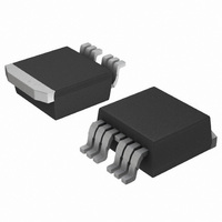
D Pak - 7 Pin Package Outline Dimensions are shown in millimeters (inches) 8 www.irf.com ...

Page 9

D Pak - 7 Pin Part Marking Information 2 D Pak - 7 Pin Tape and Reel IR WORLD HEADQUARTERS: 233 Kansas St., El Segundo, California 90245, USA Tel: (310) 252-7105 www.irf.com Data and specifications subject to change without ...

Related keywords