NTF5P03T3G ON Semiconductor, NTF5P03T3G Datasheet - Page 2
NTF5P03T3G
Manufacturer Part Number
NTF5P03T3G
Description
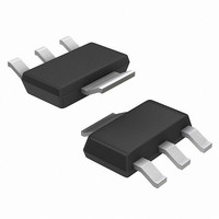
MOSFET P-CH 30V 3.7A SOT223
Manufacturer
ON Semiconductor
Datasheet
1.NTF5P03T3G.pdf
(7 pages)
Specifications of NTF5P03T3G
Fet Type
MOSFET P-Channel, Metal Oxide
Fet Feature
Logic Level Gate
Rds On (max) @ Id, Vgs
100 mOhm @ 5.2A, 10V
Drain To Source Voltage (vdss)
30V
Current - Continuous Drain (id) @ 25° C
3.7A
Vgs(th) (max) @ Id
3V @ 250µA
Gate Charge (qg) @ Vgs
38nC @ 10V
Input Capacitance (ciss) @ Vds
950pF @ 25V
Power - Max
1.56W
Mounting Type
Surface Mount
Package / Case
SOT-223 (3 leads + Tab), SC-73, TO-261
Configuration
Single Dual Drain
Transistor Polarity
P-Channel
Resistance Drain-source Rds (on)
0.1 Ohms
Forward Transconductance Gfs (max / Min)
3.9 S
Drain-source Breakdown Voltage
- 30 V
Gate-source Breakdown Voltage
+/- 20 V
Continuous Drain Current
- 5.2 A
Power Dissipation
3.13 W
Maximum Operating Temperature
+ 150 C
Mounting Style
SMD/SMT
Minimum Operating Temperature
- 55 C
Lead Free Status / RoHS Status
Lead free / RoHS Compliant
Other names
NTF5P03T3GOS
NTF5P03T3GOS
NTF5P03T3GOSTR
NTF5P03T3GOS
NTF5P03T3GOSTR
Available stocks
Company
Part Number
Manufacturer
Quantity
Price
Company:

Part Number:
NTF5P03T3G
Manufacturer:
ON
Quantity:
2 195
Company:
Part Number:
NTF5P03T3G
Manufacturer:
ON
Quantity:
30 000
Part Number:
NTF5P03T3G
Manufacturer:
ON/安森美
Quantity:
20 000


Stresses exceeding Maximum Ratings may damage the device. Maximum Ratings are stress ratings only. Functional operation above the
Recommended Operating Conditions is not implied. Extended exposure to stresses above the Recommended Operating Conditions may affect
device reliability.
1. Repetitive rating; pulse width limited by maximum junction temperature.
MAXIMUM RATINGS
Negative sign for P−Channel devices omitted for clarity
1 sq in
FR−4 or G−10 PCB
10 seconds
Minimum
FR−4 or G−10 PCB
10 seconds
Drain−to−Source Voltage
Drain−to−Gate Voltage (R
Gate−to−Source Voltage − Continuous
Operating and Storage Temperature Range
Single Pulse Drain−to−Source Avalanche Energy − Starting T
(V
DD
= −30 Vdc, V
GS
(T
= −10 Vdc, Peak I
GS
J
Thermal Resistance − Junction to Ambient
Total Power Dissipation @ T
Linear Derating Factor
Drain Current − Continuous @ T
Continuous @ T
Pulsed Drain Current (Note 1)
Thermal Resistance − Junction to Ambient
= 25°C unless otherwise noted)
= 1.0 MW)
Total Power Dissipation @ T
Linear Derating Factor
Drain Current − Continuous @ T
Continuous @ T
Pulsed Drain Current (Note 1)
Rating
L
A
= −12 Apk, L = 3.5 mH, R
= 70°C
A
= 70°C
A
= 25°C
http://onsemi.com
A
A
NTF5P03T3
= 25°C
= 25°C
J
A
= 25°C
= 25°C
2
G
= 25 W)
Symbol
T
R
R
V
V
J
V
E
I
I
THJA
P
THJA
P
DGR
, T
DSS
DM
DM
I
I
I
I
GS
D
D
D
D
AS
D
D
stg
− 55 to 150
Max
± 20
3.13
−5.2
−4.1
1.56
12.5
−3.7
−2.9
−30
−30
−26
−19
250
40
25
80
mW/°C
mW/°C
Watts
Watts
°C/W
°C/W
Unit
mJ
°C
V
V
V
A
A
A
A
A
A
Related parts for NTF5P03T3G
Image
Part Number
Description
Manufacturer
Datasheet
Request
R

Part Number:
Description:
ON Semiconductor [VOLTAGE REGULATOR]
Manufacturer:
ON Semiconductor
Datasheet:
Part Number:
Description:
357-036-542-201 CARDEDGE 36POS DL .156 BLK LOPRO
Manufacturer:
ON Semiconductor
Datasheet:
Part Number:
Description:
357-036-542-201 CARDEDGE 36POS DL .156 BLK LOPRO
Manufacturer:
ON Semiconductor
Datasheet:
Part Number:
Description:
357-036-542-201 CARDEDGE 36POS DL .156 BLK LOPRO
Manufacturer:
ON Semiconductor
Datasheet:
Part Number:
Description:
357-036-542-201 CARDEDGE 36POS DL .156 BLK LOPRO
Manufacturer:
ON Semiconductor
Datasheet:
Part Number:
Description:
357-036-542-201 CARDEDGE 36POS DL .156 BLK LOPRO
Manufacturer:
ON Semiconductor
Datasheet:
Part Number:
Description:
357-036-542-201 CARDEDGE 36POS DL .156 BLK LOPRO
Manufacturer:
ON Semiconductor
Datasheet:
Part Number:
Description:
357-036-542-201 CARDEDGE 36POS DL .156 BLK LOPRO
Manufacturer:
ON Semiconductor
Datasheet:
Part Number:
Description:
357-036-542-201 CARDEDGE 36POS DL .156 BLK LOPRO
Manufacturer:
ON Semiconductor
Datasheet:
Part Number:
Description:
357-036-542-201 CARDEDGE 36POS DL .156 BLK LOPRO
Manufacturer:
ON Semiconductor
Datasheet:
Part Number:
Description:
357-036-542-201 CARDEDGE 36POS DL .156 BLK LOPRO
Manufacturer:
ON Semiconductor
Datasheet:
Part Number:
Description:
Manufacturer:
ON Semiconductor
Datasheet:
Part Number:
Description:
Manufacturer:
ON Semiconductor
Datasheet:
Part Number:
Description:
Manufacturer:
ON Semiconductor
Datasheet: