NDF05N50ZG ON Semiconductor, NDF05N50ZG Datasheet
NDF05N50ZG
Specifications of NDF05N50ZG
Available stocks


Related parts for NDF05N50ZG

NDF05N50ZG Summary of contents
Page 1
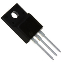
NDF05N50Z, NDP05N50Z, NDD05N50Z N-Channel Power MOSFET 500 V, 1.25 W Features • Low ON Resistance • Low Gate Charge • 100% Avalanche Tested • These Devices are Pb−Free and are RoHS Compliant ABSOLUTE MAXIMUM RATINGS (T Rating Symbol Drain−to−Source Voltage ...
Page 2
THERMAL RESISTANCE Parameter Junction−to−Case (Drain) Junction−to−Ambient Steady State 3. Insertion mounted 4. Surface mounted on FR4 board using 1″ sq. pad size, (Cu area = 1.127 oz] including traces). ELECTRICAL CHARACTERISTICS Characteristic OFF CHARACTERISTICS Drain−to−Source Breakdown Voltage ...
Page 3
8.0 7.0 6.0 5.0 4.0 3.0 2.0 1.0 0 DRAIN−TO−SOURCE VOLTAGE (V) DS Figure 1. On−Region Characteristics 2.50 2.25 2.00 1.75 1.50 1.25 1.00 ...
Page 4
T = 150°C J 1.0 0 100 150 200 250 300 350 400 450 500 V , DRAIN−TO−SOURCE VOLTAGE (V) DS Figure 7. Drain−to−Source Leakage Current versus Voltage 15.0 14.0 13.0 12.0 11.0 10.0 9.0 8.0 7.0 ...
Page 5
SINGLE PULSE T = 25° 0.1 R LIMIT DS(on) THERMAL LIMIT PACKAGE LIMIT 0.01 0 DRAIN−TO−SOURCE VOLTAGE (V) DS Figure 12. Maximum ...
Page 6
... Additional tests on slotted 4−40 screws indicate that the screw slot fails between package. However, in order to positively ensure the package integrity of the fully isolated device, ON Semiconductor does not . recommend exceeding 10 in lbs of mounting torque under any mounting conditions ...
Page 7
... ORDERING INFORMATION Order Number NDF05N50ZG NDP05N50ZG NDD05N50Z−1G NDD05N50ZT4G †For information on tape and reel specifications, including part orientation and tape sizes, please refer to our Tape and Reel Packaging Specifications Brochure, BRD8011/D. NDF05N50ZG or NDP05N50ZG AYWW Gate Drain Package TO−220FP (Pb−Free) TO−220AB (Pb−Free) IPAK (Pb− ...
Page 8
PACKAGE DIMENSIONS −B− −Y− 0.25 (0.010 ...
Page 9
... 0.13 (0.005) M *For additional information on our Pb−Free strategy and soldering details, please download the ON Semiconductor Soldering and Mounting Techniques Reference Manual, SOLDERRM/ −T− SEATING K PLANE 0.13 (0.005) M PACKAGE DIMENSIONS DPAK CASE 369AA−01 ISSUE A −T− SEATING PLANE SOLDERING FOOTPRINT ...
Page 10
... Opportunity/Affirmative Action Employer. This literature is subject to all applicable copyright laws and is not for resale in any manner. PUBLICATION ORDERING INFORMATION LITERATURE FULFILLMENT: Literature Distribution Center for ON Semiconductor P.O. Box 5163, Denver, Colorado 80217 USA Phone: 303−675−2175 or 800−344−3860 Toll Free USA/Canada Fax: 303− ...