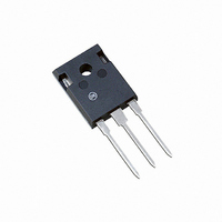
MTW32N20E ON Semiconductor, MTW32N20E Datasheet - Page 3

MTW32N20E
Manufacturer Part Number
MTW32N20E
Description
MOSFET N-CH 200V 32A TO-247
Manufacturer
ON Semiconductor
Datasheet
1.MTW32N20EG.pdf
(7 pages)
Specifications of MTW32N20E
Fet Type
MOSFET N-Channel, Metal Oxide
Fet Feature
Standard
Rds On (max) @ Id, Vgs
75 mOhm @ 16A, 10V
Drain To Source Voltage (vdss)
200V
Current - Continuous Drain (id) @ 25° C
32A
Vgs(th) (max) @ Id
4V @ 250µA
Gate Charge (qg) @ Vgs
120nC @ 10V
Input Capacitance (ciss) @ Vds
5000pF @ 25V
Power - Max
180W
Mounting Type
Through Hole
Package / Case
TO-247-3 (Straight Leads), TO-247AC
Lead Free Status / RoHS Status
Contains lead / RoHS non-compliant
Other names
MTW32N20EOS
Available stocks
Company
Part Number
Manufacturer
Quantity
Price
Company:
Part Number:
MTW32N20E
Manufacturer:
ON
Quantity:
12 500
Part Number:
MTW32N20E
Manufacturer:
MOTOROLA/摩托罗拉
Quantity:
20 000
Company:
Part Number:
MTW32N20EG
Manufacturer:
NXP
Quantity:
2 000
0.16
0.14
0.12
0.08
0.06
0.04
0.02
100
0.1
2.5
1.5
0.5
80
60
40
20
0
0
2
1
-50
0
0
Figure 3. On−Resistance versus Drain Current
V
GS
-25
Figure 5. On−Resistance Variation with
8
Figure 1. On−Region Characteristics
= 10 V
V
V
I
D
T
DS
GS
2
J
= 16 A
= 25°C
, DRAIN-TO-SOURCE VOLTAGE (VOLTS)
16
= 10 V
0
T
J
, JUNCTION TEMPERATURE (°C)
I
D
, DRAIN CURRENT (AMPS)
and Temperature
24
25
Temperature
4
T
J
32
50
= 100°C
- 55°C
25°C
TYPICAL ELECTRICAL CHARACTERISTICS
6
40
75
V
GS
= 10 V
100
48
8
125
http://onsemi.com
56
9 V
8 V
7 V
6 V
5 V
150
10
64
3
10000
2000
1000
0.09
0.08
0.07
0.06
0.05
200
100
0.1
50
40
30
20
10
20
10
0
0
0
0
Figure 4. On−Resistance versus Drain Current
100°C
V
GS
T
J
8
= 0 V
Figure 6. Drain−To−Source Leakage
= 125°C
Figure 2. Transfer Characteristics
V
V
DS
V
2
GS
DS
, DRAIN-TO-SOURCE VOLTAGE (VOLTS)
, GATE-TO-SOURCE VOLTAGE (VOLTS)
16
50
25°C
≥ 10 V
Current versus Voltage
I
D
, DRAIN CURRENT (AMPS)
and Gate Voltage
24
4
100
32
T
J
V
= - 55°C
GS
6
40
= 10 V
15 V
150
48
8
T
J
100°C
25°C
= 25°C
56
200
10
64


