MTD6N15T4 ON Semiconductor, MTD6N15T4 Datasheet
MTD6N15T4
Specifications of MTD6N15T4
Available stocks


Related parts for MTD6N15T4

MTD6N15T4 Summary of contents
Page 1
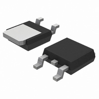
... Pb−Free Package ORDERING INFORMATION Device Package Shipping MTD6N15T4 DPAK 2500/Tape & Reel MTD6N15T4G DPAK 2500/Tape & Reel (Pb−Free) †For information on tape and reel specifications, including part orientation and tape sizes, please refer to our Tape and Reel Packaging Specification Brochure, BRD8011/D. ...
Page 2
ELECTRICAL CHARACTERISTICS Characteristic OFF CHARACTERISTICS Drain−Source Breakdown Voltage ( Vdc Zero Gate Voltage Drain Current (V = Rated Vdc) DS DSS 125°C J Gate−Body Leakage Current, Forward (V ...
Page 3
TYPICAL ELECTRICAL CHARACTERISTICS DRAIN−TO−SOURCE VOLTAGE (VOLTS) DS Figure 2. On−Region Characteristics 14 V ...
Page 4
R LIMIT 0.5 DS(on) THERMAL LIMIT PACKAGE LIMIT 0.2 0 25° SINGLE PULSE GS 0.05 0.03 0.3 0.5 0 ...
Page 5
400 GATE−TO−SOURCE OR DRAIN−TO−SOURCE VOLTAGE (VOLTS) Figure 11. Capacitance Variation V in PULSE GENERATOR gen ...
Page 6
... G 0.13 (0.005) *For additional information on our Pb−Free strategy and soldering details, please download the ON Semiconductor Soldering and Mounting Techniques Reference Manual, SOLDERRM/D. ON Semiconductor and are registered trademarks of Semiconductor Components Industries, LLC (SCILLC). SCILLC reserves the right to make changes without further notice to any products herein ...