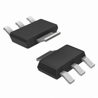
NTF3055-100T3LF ON Semiconductor, NTF3055-100T3LF Datasheet - Page 3

NTF3055-100T3LF
Manufacturer Part Number
NTF3055-100T3LF
Description
MOSFET N-CH 60V 3A SOT223
Manufacturer
ON Semiconductor
Datasheet
1.NTF3055-100T1G.pdf
(6 pages)
Specifications of NTF3055-100T3LF
Fet Type
MOSFET N-Channel, Metal Oxide
Fet Feature
Logic Level Gate
Rds On (max) @ Id, Vgs
110 mOhm @ 1.5A, 10V
Drain To Source Voltage (vdss)
60V
Current - Continuous Drain (id) @ 25° C
3A
Vgs(th) (max) @ Id
4V @ 250µA
Gate Charge (qg) @ Vgs
22nC @ 10V
Input Capacitance (ciss) @ Vds
455pF @ 25V
Power - Max
1.3W
Mounting Type
Surface Mount
Package / Case
SOT-223 (3 leads + Tab), SC-73, TO-261
Lead Free Status / RoHS Status
Contains lead / RoHS non-compliant
Other names
NTF3055-100T3LFOS
0.16
0.14
0.12
0.08
0.06
0.04
0.02
0.1
2.2
1.8
1.6
1.4
1.2
0.8
0.6
6
5
4
3
2
0
−50
1
0
2
1
0
0
V
GS
I
V
D
GS
−25
V
= 1.5 A
Figure 5. On−Resistance Variation with
= 10 V
DS,
Figure 1. On−Region Characteristics
= 10 V
1
DRAIN−TO−SOURCE VOLTAGE (VOLTS)
Figure 3. On−Resistance versus
T
J
V
0
, JUNCTION TEMPERATURE (°C)
GS
1
I
V
D,
Gate−to−Source Voltage
GS
= 8 V
DRAIN CURRENT (AMPS)
25
2
= 10 V
V
Temperature
GS
T
T
T
J
J
50
= 6 V
J
= 100°C
= −55°C
= 25°C
3
2
75
100
4
V
3
GS
V
V
125
GS
GS
= 4.5 V
5
= 4 V
= 5 V
150
http://onsemi.com
175
4
6
3
1000
0.16
0.14
0.12
0.08
0.06
0.04
0.02
100
0.1
10
5
4
1
0
1
6
3
2
0
0
3
0
Figure 4. On−Resistance versus Drain Current
V
Figure 6. Drain−to−Source Leakage Current
V
GS
V
GS
T
V
DS
V
J
DS,
= 0 V
GS,
= 15 V
= 100°C
3.5
Figure 2. Transfer Characteristics
10
≥ 10 V
1
DRAIN−TO−SOURCE VOLTAGE (VOLTS)
T
GATE−TO−SOURCE VOLTAGE (VOLTS)
J
= 25°C
I
D,
DRAIN CURRENT (AMPS)
20
and Gate Voltage
4
2
versus Voltage
T
T
T
J
J
J
T
T
T
= 150°C
= 125°C
= 100°C
J
J
J
= 25°C
= 100°C
= −55°C
4.5
30
T
3
J
= −55°C
40
5
4
5.5
50
5
60
6
6


