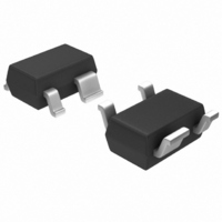
ATF-35143-BLKG Avago Technologies US Inc., ATF-35143-BLKG Datasheet - Page 4

ATF-35143-BLKG
Manufacturer Part Number
ATF-35143-BLKG
Description
IC PHEMT 1.9GHZ 15MA LN SOT-343
Manufacturer
Avago Technologies US Inc.
Datasheet
1.ATF-35143-BLKG.pdf
(19 pages)
Specifications of ATF-35143-BLKG
Package / Case
SC-70-4, SC-82-4, SOT-323-4, SOT-343
Transistor Type
pHEMT FET
Frequency
2GHz
Gain
18dB
Voltage - Rated
5.5V
Current Rating
80mA
Noise Figure
0.4dB
Current - Test
15mA
Voltage - Test
2V
Power - Output
10dBm
Configuration
Single Dual Source
Transistor Polarity
N-Channel
Power Dissipation
300 mW
Drain Source Voltage Vds
5.5 V
Gate-source Breakdown Voltage
- 5 V
Continuous Drain Current
80 mA
Maximum Operating Temperature
+ 160 C
Maximum Drain Gate Voltage
- 5 V
Minimum Operating Temperature
- 65 C
Mounting Style
SMD/SMT
Power Dissipation Pd
300mW
Noise Figure Typ
0.4dB
Rf Transistor Case
SOT-343
No. Of Pins
4
Drain Current Idss Max
15mA
Drain-source Breakdown Voltage
5.5V
Rohs Compliant
Yes
Lead Free Status / RoHS Status
Lead free / RoHS Compliant
Lead Free Status / RoHS Status
Lead free / RoHS Compliant, Lead free / RoHS Compliant
Other names
516-1864
ATF-35143-BLKG
ATF-35143-BLKG
Available stocks
Company
Part Number
Manufacturer
Quantity
Price
Part Number:
ATF-35143-BLKG
Manufacturer:
AVAGO/安华高
Quantity:
20 000
ATF-35143 Typical Performance Curves
Notes:
1. Measurements made on a fixed tuned production test board that was tuned for optimal gain match with reasonable noise figure at 2 V 15 mA
2. P
4
Figure 6. OIP3 and P
Figure 8. NF and G
Figure 10. P
Tuned for NF @ 2V, 15 mA at 2 GHz.
30
25
20
15
10
20
19
18
17
16
15
25
20
15
10
-5
bias. This circuit represents a trade-off between optimal noise match, maximum gain match and a realizable match based on production test
board requirements. Circuit losses have been de-embedded from actual measurements.
current may increase or decrease depending on frequency and dc bias point. At lower values of I
output approaches P
current source as is typically done with active biasing. As an example, at a V
approached.
5
0
5
0
1dB
0
0
0
measurements are performed with passive biasing. Quiescent drain current, I
OIP3
10
10
1dB
G
vs. Bias (Active Bias)
20
a
a
20
20
vs. Bias at 2 GHz.
1dB
I
I
DSQ
DSQ
I
DS
vs. Bias at 2 GHz.
30
30
40
(mA)
1dB
(mA)
(mA)
NF
. This results in higher P
40
40
[1]
[1]
P
60
1dB
[1,2]
50
50
2 V
3 V
4 V
2 V
3 V
4 V
2 V
3 V
4 V
60
60
80
2.5
2
1.5
1
0.5
0
1dB
and higher PAE (power added efficiency) when compared to a device that is driven by a constant
Figure 11. P
Tuned for NF @ 2V, 15 mA at 900 MHz.
Figure 7. OIP3 and P
Figure 9. NF and G
30
25
20
15
10
24
22
20
18
16
14
20
15
10
-5
5
5
0
0
0
0
OIP3
10
10
1dB
G
vs. Bias (Active Bias)
20
a
a
20
20
vs. Bias at 900 MHz.
1dB
DS
I
I
DSQ
DSQ
I
DS
vs. Bias at 900 MHz.
= 4 V and I
DSQ
30
30
40
(mA)
(mA)
(mA)
, is set with zero RF drive applied. As P
NF
40
40
P
1dB
DSQ
60
[1]
[1]
50
50
= 5 mA, I
[1,2]
2 V
3 V
4 V
2 V
3 V
4 V
2 V
3 V
4 V
DSQ
60
60
80
the device is running closer to class B as power
2.5
2
1.5
1
0.5
0
d
increases to 30 mA as a P
1dB
is approached, the drain
1dB
of +15 dBm is


