MW6S010NR1 Freescale Semiconductor, MW6S010NR1 Datasheet - Page 19
MW6S010NR1
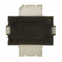
Manufacturer Part Number
MW6S010NR1
Description
MOSFET RF N-CH 28V 10W TO-270-2
Manufacturer
Freescale Semiconductor
Datasheet
1.MW6S010NR1.pdf
(20 pages)
Specifications of MW6S010NR1
Transistor Type
N-Channel
Frequency
960MHz
Gain
18dB
Voltage - Rated
68V
Current Rating
10µA
Current - Test
125mA
Voltage - Test
28V
Power - Output
10W
Package / Case
TO-270-2
Configuration
Dual
Transistor Polarity
N-Channel
Drain-source Breakdown Voltage
68 V
Gate-source Breakdown Voltage
12 V
Continuous Drain Current
125 mA
Power Dissipation
10 W
Maximum Operating Temperature
+ 150 C
Mounting Style
SMD/SMT
Minimum Operating Temperature
- 65 C
Channel Type
N
Channel Mode
Enhancement
Drain Source Voltage (max)
68V
Power Gain (typ)@vds
20dB
Frequency (max)
1.5GHz
Package Type
TO-270
Pin Count
3
Output Capacitance (typ)@vds
10@28VpF
Reverse Capacitance (typ)
0.32@28VpF
Operating Temp Range
-65C to 225C
Drain Efficiency (typ)
33%
Mounting
Surface Mount
Mode Of Operation
2-Tone
Number Of Elements
1
Power Dissipation (max)
61400mW
Vswr (max)
10
Screening Level
Military
Drain Source Voltage Vds
68V
Rf Transistor Case
TO-270
Msl
MSL 3 - 168 Hours
Filter Terminals
SMD
Peak Reflow Compatible (260 C)
Yes
Rohs Compliant
Yes
Operating Frequency Max
900MHz
Gate-source Voltage
12V
Leaded Process Compatible
Yes
Lead Free Status / RoHS Status
Lead free / RoHS Compliant
Noise Figure
-
Lead Free Status / Rohs Status
Lead free / RoHS Compliant
Other names
MW6S010NR1
MW6S010NR1TR
MW6S010NR1TR
Available stocks
Company
Part Number
Manufacturer
Quantity
Price
Company:

Part Number:
MW6S010NR1
Manufacturer:
OMRON
Quantity:
2 300
Part Number:
MW6S010NR1
Manufacturer:
FREESCALE
Quantity:
20 000


RF Device Data
Freescale Semiconductor
Application Notes
• AN1907: Solder Reflow Attach Method for High Power RF Devices in Plastic Packages
• AN1949: Mounting Method for the MHVIC910HR2 (PFP - 16) and Similar Surface Mount Packages
• AN1955: Thermal Measurement Methodology of RF Power Amplifiers
• AN3789: Clamping of High Power RF Transistors and RFICs in Over - Molded Plastic Packages
Engineering Bulletins
• EB212: Using Data Sheet Impedances for RF LDMOS Devices
Software
• Electromigration MTTF Calculator
• RF High Power Model
For Software and Tools, do a Part Number search at http://www.freescale.com, and select the “Part Number” link. Go to the
Software & Tools tab on the part’s Product Summary page to download the respective tool.
Revision
Refer to the following documents to aid your design process.
The following table summarizes revisions to this document.
4
5
June 2009
Dec. 2008
Date
• Changed Storage Temperature Range in Max Ratings table from - 65 to +175 to - 65 to +150 for
• Removed Total Device Dissipation from Max Ratings table as data was redundant (information already
• Added Case Operating Temperature limit to the Maximum Ratings table and set limit to 150°C, p. 1
• Operating Junction Temperature increased from 200°C to 225°C in Maximum Ratings table, related
• Corrected V
• Corrected C
• Updated Part Numbers in Tables 6, 7, Component Designations and Values, to RoHS compliant part
• Removed lower voltage tests from Fig. 10, Power Gain versus Output Power, due to fixed tuned fixture
• Replaced Fig. 12, MTTF versus Junction Temperature with updated graph. Removed Amps
• Replaced Case Outline 1265 - 08 with 1265 - 09, Issue K, p. 1, 13 - 15. Corrected cross hatch pattern in
• Replaced Case Outline 1265A - 02 with 1265A - 03, Issue C, p. 1, 16 - 18. Corrected cross hatch pattern and
• Added Product Documentation and Revision History, p. 19
• Modified data sheet to reflect MSL rating change from 1 to 3 as a result of the standardization of packing
• Added AN3789, Clamping of High Power RF Transistors and RFICs in Over - Molded Plastic Packages to
• Added Electromigration MTTF Calculator and RF High Power Model availability to Product Software, p. 19
standardization across products, p. 1
provided in Thermal Characteristics table), p. 1
“Continuous use at maximum temperature will affect MTTF” footnote added and changed 200°C to 225°C in
Capable Plastic Package bullet, p. 1
Test”, On Characteristics table, p. 2
Dynamic Characteristics table, p. 2
numbers, p. 3, 9
limitations, p. 6
operating characteristics and location of MTTF calculator for device, p. 7
bottom view and changed its dimensions (D2 and E3) to minimum value on source contact (D2 changed
from Min - Max .290 - .320 to .290 Min; E3 changed from Min - Max .150 - .180 to .150 Min). Added JEDEC
Standard Package Number.
its dimensions (D2 and E2) on source contact (D2 changed from Min - Max .290 - .320 to .290 Min; E3
changed from Min - Max .150 - .180 to .150 Min). Added pin numbers. Corrected mm dimension L for
gull - wing foot from 4.90 - 5.06 Min - Max to 0.46 - 0.61 Min - Max. Added JEDEC Standard Package Number.
process as described in Product and Process Change Notification number, PCN13516, p. 2
Product Documentation, Application Notes, p. 19
PRODUCT DOCUMENTATION, TOOLS AND SOFTWARE
DS
iss
to V
test condition to indicate AC stimulus on the V
DD
in the RF test condition voltage callout for V
REVISION HISTORY
Description
GS
connection versus the V
GS(Q)
and added “Measured in Functional
MW6S010NR1 MW6S010GNR1
DS
2
connection,
and listed
19
Related parts for MW6S010NR1
Image
Part Number
Description
Manufacturer
Datasheet
Request
R

Part Number:
Description:
RF Power Field Effect Transistor
Manufacturer:
Freescale Semiconductor
Datasheet:


Part Number:
Description:
RELAY HI FREQ 6GHZ DPDT
Manufacturer:
TE Connectivity
Datasheet:

Part Number:
Description:
Manufacturer:
Freescale Semiconductor, Inc
Datasheet:
Part Number:
Description:
Manufacturer:
Freescale Semiconductor, Inc
Datasheet:
Part Number:
Description:
Manufacturer:
Freescale Semiconductor, Inc
Datasheet:
Part Number:
Description:
Manufacturer:
Freescale Semiconductor, Inc
Datasheet:
Part Number:
Description:
Manufacturer:
Freescale Semiconductor, Inc
Datasheet:
Part Number:
Description:
Manufacturer:
Freescale Semiconductor, Inc
Datasheet:
Part Number:
Description:
Manufacturer:
Freescale Semiconductor, Inc
Datasheet:
Part Number:
Description:
Manufacturer:
Freescale Semiconductor, Inc
Datasheet:
Part Number:
Description:
Manufacturer:
Freescale Semiconductor, Inc
Datasheet:
Part Number:
Description:
Manufacturer:
Freescale Semiconductor, Inc
Datasheet:
Part Number:
Description:
Manufacturer:
Freescale Semiconductor, Inc
Datasheet:
Part Number:
Description:
Manufacturer:
Freescale Semiconductor, Inc
Datasheet: