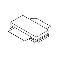
MRF6S19100HSR3 Freescale Semiconductor, MRF6S19100HSR3 Datasheet

MRF6S19100HSR3
Specifications of MRF6S19100HSR3
Available stocks
Related parts for MRF6S19100HSR3
MRF6S19100HSR3 Summary of contents
Page 1
... MHz AVG CDMA LATERAL N - CHANNEL RF POWER MOSFETs CASE 465 - 06, STYLE 780 MRF6S19100HR3 CASE 465A - 06, STYLE 780S MRF6S19100HSR3 Symbol Value Unit V - 0.5, +68 Vdc DSS V - 0.5, +12 Vdc +150 °C stg T 150 ° 225 °C J (2,3) Symbol Value Unit R °C/W θJC 0.44 0.50 MRF6S19100HR3 MRF6S19100HSR3 1 ...
Page 2
... N - CDMA, 1.2288 MHz Channel Bandwidth Carriers. ACPR measured in 30 kHz Channel Bandwidth @ ±885 kHz Offset. IM3 measured in 1.2288 MHz Channel Bandwidth @ ±2.5 MHz Offset. PAR = 9 0.01% Probability on CCDF. Power Gain Drain Efficiency Intermodulation Distortion Adjacent Channel Power Ratio Input Return Loss 1. Part is internally matched both on input and output. MRF6S19100HR3 MRF6S19100HSR3 2 = 25°C unless otherwise noted) C Symbol I DSS I ...
Page 3
... ATC100B150CT500XT ATC100B5R6JT500XT T491C105K050AT ATC100B430CT500XT T491X226K035AT T491C106K035AT C1825C14J5RAC MCHT101M1HB- 1017 - RH CRCW120612R0FKEA CRCW12062001FKEA V SUPPLY + + + + C10 C11 C12 OUTPUT Z8 Z9 Z10 Z11 C6 = 2.55 r Part Number Manufacturer Fair - Rite Johanson Dielectrics ATC ATC Kemet ATC Kemet Kemet Kemet Multicomp Vishay Vishay MRF6S19100HR3 MRF6S19100HSR3 RF 3 ...
Page 4
... Freescale has begun the transition of marking Printed Circuit Boards (PCBs) with the Freescale Semiconductor signature/logo. PCBs may have either Motorola or Freescale markings during the transition period. These changes will have no impact on form, fit or function of the current product. Figure 2. MRF6S19100HR3(HSR3) Test Circuit Component Layout MRF6S19100HR3 MRF6S19100HSR3 ...
Page 5
... Watts Avg. out −25 −5 −30 −10 −35 −15 −40 −20 −45 1980 1990 = 44 Watts Avg. out = 28 Vdc 1958.75 MHz 1961.25 MHz I = 450 mA 675 mA DQ 1125 mA 900 mA 10 100 P , OUTPUT POWER (WATTS) PEP out versus Output Power MRF6S19100HR3 MRF6S19100HSR3 300 5 ...
Page 6
... Probability (CCDF Figure Carrier N - CDMA ACPR, IM3, Power Gain η OUTPUT POWER (WATTS) CW out Figure 10. Power Gain and Drain Efficiency versus CW Output Power MRF6S19100HR3 MRF6S19100HSR3 6 TYPICAL CHARACTERISTICS P1dB = 50.9 dBm (124 100 30 31 Figure 8. Pulsed CW Output Power versus = 28 Vdc 900 100 P , OUTPUT POWER (WATTS) AVG ...
Page 7
... Figure 14 Carrier N - CDMA Spectrum 230 250 = 28%. 1.2288 MHz Channel BW −IM3 in +IM3 in 1.2288 MHz 1.2288 MHz Integrated BW Integrated BW −ACPR in 30 kHz +ACPR in 30 kHz Integrated BW Integrated BW −4.5 −3 −1.5 0 1.5 3 4.5 f, FREQUENCY (MHz) MRF6S19100HR3 MRF6S19100HSR3 6 7.5 7 ...
Page 8
... Figure 15. Series Equivalent Source and Load Impedance MRF6S19100HR3 MRF6S19100HSR3 1990 MHz f = 1930 MHz Z load f = 1990 MHz = 5 Ω 1930 MHz Vdc 900 mA Avg out source load MHz Ω Ω 1930 1.57 - j3.50 2.26 - j2.31 1960 1.83 - j3.29 2.22 - j2.13 1990 2.34 - j3.71 2 ...
Page 9
... REF 0.127 REF F bbb 0.010 REF 0.254 REF ccc 0.015 REF 0.381 REF STYLE 1: PIN 1. DRAIN 2. GATE 5. SOURCE MRF6S19100HR3 MRF6S19100HSR3 MAX 34.16 9.91 4.32 12.83 1.14 0.15 1.70 5.33 19.96 20.00 3.51 9.53 9.52 9 ...
Page 10
... Removed lower voltage tests from Fig. 11, Power Gain versus Output Power, due to fixed tuned fixture limitations • Replaced Fig. 12, MTTF versus Junction Temperature with updated graph. Removed Amps operating characteristics and location of MTTF calculator for device • Added Product Documentation and Revision History MRF6S19100HR3 MRF6S19100HSR3 10 PRODUCT DOCUMENTATION REVISION HISTORY Description ...
Page 11
... Semiconductor was negligent regarding the design or manufacture of the part. Freescalet and the Freescale logo are trademarks of Freescale Semiconductor, Inc. All other product or service names are the property of their respective owners. © Freescale Semiconductor, Inc. 2004 - 2006, 2008. All rights reserved. MRF6S19100HR3 MRF6S19100HSR3 11 ...


