MRF6VP41KHR6 Freescale Semiconductor, MRF6VP41KHR6 Datasheet - Page 2
MRF6VP41KHR6
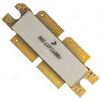
Manufacturer Part Number
MRF6VP41KHR6
Description
MOSFET RF N-CH 1000W NI1230
Manufacturer
Freescale Semiconductor
Datasheet
1.MRF6VP41KHR7.pdf
(18 pages)
Specifications of MRF6VP41KHR6
Transistor Type
2 N-Channel (Dual)
Frequency
450MHz
Gain
20dB
Voltage - Rated
110V
Current Rating
5mA
Current - Test
150mA
Voltage - Test
50V
Power - Output
1000W
Package / Case
NI-1230
Drain Source Voltage Vds
110V
Continuous Drain Current Id
5mA
Power Dissipation Pd
1kW
Operating Temperature Range
-65°C To +150°C
Rf Transistor Case
NI-1230
No. Of Pins
4
Rohs Compliant
Yes
Lead Free Status / RoHS Status
Lead free / RoHS Compliant
Noise Figure
-


2
MRF6VP41KHR6 MRF6VP41KHSR6
Table 2. Thermal Characteristics
Table 3. ESD Protection Characteristics
Table 4. Electrical Characteristics
Off Characteristics
On Characteristics
Dynamic Characteristics
Functional Tests
100 μsec Pulse Width, 20% Duty Cycle
1. MTTF calculator available at http://www.freescale.com/rf. Select Software & Tools/Development Tools/Calculators to access MTTF
2. Refer to AN1955, Thermal Measurement Methodology of RF Power Amplifiers. Go to http://www.freescale.com/rf.
3. Each side of device measured separately.
4. Measurement made with device in push--pull configuration.
Thermal Resistance, Junction to Case
Human Body Model (per JESD22--A114)
Machine Model (per EIA/JESD22--A115)
Charge Device Model (per JESD22--C101)
Gate--Source Leakage Current
Drain--Source Breakdown Voltage
Zero Gate Voltage Drain Leakage Current
Zero Gate Voltage Drain Leakage Current
Gate Threshold Voltage
Gate Quiescent Voltage
Drain--Source On--Voltage
Reverse Transfer Capacitance
Output Capacitance
Input Capacitance
Power Gain
Drain Efficiency
Input Return Loss
Case Temperature 80°C, 1000 W Pulsed, 100 μsec Pulse Width, 20% Duty Cycle, 450 MHz
Case Temperature 48°C, 1000 W CW, 352.2 MHz
(V
(I
(V
(V
(V
(V
(V
(V
(V
(V
calculators by product.
Select Documentation/Application Notes -- AN1955.
D
GS
DS
DS
DS
DD
GS
DS
DS
DS
= 300 mA, V
= 5 Vdc, V
= 50 Vdc, V
= 100 Vdc, V
= 10 Vdc, I
= 50 Vdc, I
= 10 Vdc, I
= 50 Vdc ± 30 mV(rms)ac @ 1 MHz, V
= 50 Vdc ± 30 mV(rms)ac @ 1 MHz, V
= 50 Vdc, V
(4)
GS
DS
D
D
D
(In Freescale Test Fixture, 50 ohm system) V
(3)
GS
GS
= 1600 μAdc)
= 150 mAdc, Measured in Functional Test)
= 4 Adc)
GS
= 0 Vdc)
= 0 Vdc)
= 0 Vdc)
= 0 Vdc ± 30 mV(rms)ac @ 1 MHz)
= 0 Vdc)
(3)
(4)
(3)
(3)
Characteristic
Test Methodology
Characteristic
(T
A
= 25°C unless otherwise noted)
GS
GS
= 0 Vdc)
= 0 Vdc)
DD
= 50 Vdc, I
V
Symbol
DQ
V
V
V
(BR)DSS
I
I
I
C
DS(on)
C
GS(th)
GS(Q)
C
G
IRL
GSS
DSS
DSS
η
oss
rss
= 150 mA, P
iss
ps
D
Min
110
1.5
out
19
60
—
—
—
—
—
—
—
—
1
= 1000 W Peak (200 W Avg.), f = 450 MHz,
Symbol
R
θJC
1.68
0.28
Typ
147
506
--18
2.2
3.3
20
64
—
—
—
—
IV (Minimum)
A (Minimum)
2 (Minimum)
Class
Freescale Semiconductor
Value
0.03
0.15
Max
100
3.5
10
22
—
—
—
—
—
—
--9
(1,2)
5
3
RF Device Data
(continued)
°C/W
μAdc
μAdc
Unit
Unit
Vdc
Vdc
Vdc
Vdc
mA
dB
dB
pF
pF
pF
%
Related parts for MRF6VP41KHR6
Image
Part Number
Description
Manufacturer
Datasheet
Request
R

Part Number:
Description:
Manufacturer:
Freescale Semiconductor, Inc
Datasheet:
Part Number:
Description:
Manufacturer:
Freescale Semiconductor, Inc
Datasheet:
Part Number:
Description:
Manufacturer:
Freescale Semiconductor, Inc
Datasheet:
Part Number:
Description:
Manufacturer:
Freescale Semiconductor, Inc
Datasheet:
Part Number:
Description:
Manufacturer:
Freescale Semiconductor, Inc
Datasheet:
Part Number:
Description:
Manufacturer:
Freescale Semiconductor, Inc
Datasheet:
Part Number:
Description:
Manufacturer:
Freescale Semiconductor, Inc
Datasheet:
Part Number:
Description:
Manufacturer:
Freescale Semiconductor, Inc
Datasheet:
Part Number:
Description:
Manufacturer:
Freescale Semiconductor, Inc
Datasheet:
Part Number:
Description:
Manufacturer:
Freescale Semiconductor, Inc
Datasheet:
Part Number:
Description:
Manufacturer:
Freescale Semiconductor, Inc
Datasheet:
Part Number:
Description:
Manufacturer:
Freescale Semiconductor, Inc
Datasheet:
Part Number:
Description:
Manufacturer:
Freescale Semiconductor, Inc
Datasheet:
Part Number:
Description:
Manufacturer:
Freescale Semiconductor, Inc
Datasheet:
Part Number:
Description:
Manufacturer:
Freescale Semiconductor, Inc
Datasheet: