MRF6VP41KHR6 Freescale Semiconductor, MRF6VP41KHR6 Datasheet - Page 6
MRF6VP41KHR6
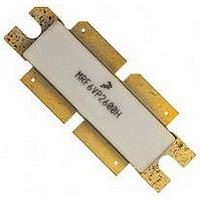
Manufacturer Part Number
MRF6VP41KHR6
Description
MOSFET RF N-CH 1000W NI1230
Manufacturer
Freescale Semiconductor
Datasheet
1.MRF6VP41KHR7.pdf
(18 pages)
Specifications of MRF6VP41KHR6
Transistor Type
2 N-Channel (Dual)
Frequency
450MHz
Gain
20dB
Voltage - Rated
110V
Current Rating
5mA
Current - Test
150mA
Voltage - Test
50V
Power - Output
1000W
Package / Case
NI-1230
Drain Source Voltage Vds
110V
Continuous Drain Current Id
5mA
Power Dissipation Pd
1kW
Operating Temperature Range
-65°C To +150°C
Rf Transistor Case
NI-1230
No. Of Pins
4
Rohs Compliant
Yes
Lead Free Status / RoHS Status
Lead free / RoHS Compliant
Noise Figure
-


6
MRF6VP41KHR6 MRF6VP41KHSR6
1000
100
23
22
21
20
19
18
17
21
20
19
18
17
16
15
14
13
10
1
Figure 4. Capacitance versus Drain- -Source Voltage
10
Figure 6. Pulsed Power Gain and Drain Efficiency
1
0
V
I
f = 450 MHz
Pulse Width = 100 μsec
Duty Cycle = 20%
DQ
I
DD
Note: Each side of device measured separately.
DQ
= 150 mA
3600 mA
= 50 Vdc
= 6000 mA
Figure 8. Pulsed Power Gain versus
C
750 mA
rss
1500 mA
375 mA
P
P
10
V
out
out
150 mA
DS
C
, OUTPUT POWER (WATTS) PULSED
, OUTPUT POWER (WATTS) PULSED
, DRAIN--SOURCE VOLTAGE (VOLTS)
iss
C
versus Output Power
10
oss
Output Power
Measured with ±30 mV(rms)ac @ 1 MHz
V
100
GS
20
= 0 Vdc
V
f = 450 MHz
Pulse Width = 100 μsec
Duty Cycle = 20%
DD
100
= 50 Vdc
30
G
ps
η
D
TYPICAL CHARACTERISTICS
40
1000
1000 2000
2000
50
80
70
60
50
40
30
20
10
0
22
20
18
16
14
12
100
65
64
63
62
61
60
59
58
57
56
55
10
34
0
1
1
Note: Each side of device measured separately.
35
T
Figure 7. Pulsed Output Power versus
C
200
Figure 9. Pulsed Power Gain versus
P1dB = 60.33 dBm (1078.94 W)
V
= 25°C
DD
Figure 5. DC Safe Operating Area
36
P
= 30 V
V
out
DS
P
, OUTPUT POWER (WATTS) PULSED
400
in
, DRAIN--SOURCE VOLTAGE (VOLTS)
37
, INPUT POWER (dBm) PULSED
P3dB = 60.70 dBm (1174.89 W)
35 V
Output Power
Input Power
38
600
40 V
39
10
T
J
800
Freescale Semiconductor
I
Pulse Width = 100 μsec
Duty Cycle = 20%
= 150°C
DQ
40
= 150 mA, f = 450 MHz
45 V
V
I
f = 450 MHz
Pulse Width = 100 μsec
Duty Cycle = 20%
DQ
DD
T
1000
41
= 150 mA
J
= 50 Vdc
= 200°C
RF Device Data
50 V
42
1200
T
Ideal
J
Actual
= 175°C
43
1400
100
44
Related parts for MRF6VP41KHR6
Image
Part Number
Description
Manufacturer
Datasheet
Request
R

Part Number:
Description:
Manufacturer:
Freescale Semiconductor, Inc
Datasheet:
Part Number:
Description:
Manufacturer:
Freescale Semiconductor, Inc
Datasheet:
Part Number:
Description:
Manufacturer:
Freescale Semiconductor, Inc
Datasheet:
Part Number:
Description:
Manufacturer:
Freescale Semiconductor, Inc
Datasheet:
Part Number:
Description:
Manufacturer:
Freescale Semiconductor, Inc
Datasheet:
Part Number:
Description:
Manufacturer:
Freescale Semiconductor, Inc
Datasheet:
Part Number:
Description:
Manufacturer:
Freescale Semiconductor, Inc
Datasheet:
Part Number:
Description:
Manufacturer:
Freescale Semiconductor, Inc
Datasheet:
Part Number:
Description:
Manufacturer:
Freescale Semiconductor, Inc
Datasheet:
Part Number:
Description:
Manufacturer:
Freescale Semiconductor, Inc
Datasheet:
Part Number:
Description:
Manufacturer:
Freescale Semiconductor, Inc
Datasheet:
Part Number:
Description:
Manufacturer:
Freescale Semiconductor, Inc
Datasheet:
Part Number:
Description:
Manufacturer:
Freescale Semiconductor, Inc
Datasheet:
Part Number:
Description:
Manufacturer:
Freescale Semiconductor, Inc
Datasheet:
Part Number:
Description:
Manufacturer:
Freescale Semiconductor, Inc
Datasheet: