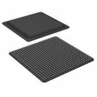
XC2V3000-4FGG676C Xilinx Inc, XC2V3000-4FGG676C Datasheet - Page 50

XC2V3000-4FGG676C
Manufacturer Part Number
XC2V3000-4FGG676C
Description
FPGA Virtex-II™ Family 3M Gates 32256 Cells 650MHz 0.15um/0.12um (CMOS) Technology 1.5V 676-Pin FBGA
Manufacturer
Xilinx Inc
Series
Virtex™-IIr
Datasheet
1.XC2V250-4FGG256C.pdf
(318 pages)
Specifications of XC2V3000-4FGG676C
Package
676FBGA
Family Name
Virtex-IIÂ
Device Logic Units
32256
Device System Gates
3000000
Number Of Registers
28672
Maximum Internal Frequency
650 MHz
Typical Operating Supply Voltage
1.5 V
Maximum Number Of User I/os
484
Ram Bits
1769472
Number Of Labs/clbs
3584
Total Ram Bits
1769472
Number Of I /o
484
Number Of Gates
3000000
Voltage - Supply
1.425 V ~ 1.575 V
Mounting Type
Surface Mount
Operating Temperature
0°C ~ 85°C
Package / Case
676-BBGA
Lead Free Status / RoHS Status
Lead free / RoHS Compliant
Number Of Logic Elements/cells
-
Lead Free Status / RoHS Status
Lead free / RoHS Compliant
Other names
122-1354
Available stocks
Company
Part Number
Manufacturer
Quantity
Price
Company:
Part Number:
XC2V3000-4FGG676C
Manufacturer:
XILINX
Quantity:
1 831
Company:
Part Number:
XC2V3000-4FGG676C
Manufacturer:
Xilinx Inc
Quantity:
10 000
- Current page: 50 of 318
- Download datasheet (3Mb)
Table 2: Recommended Operating Conditions
Table 3: DC Characteristics Over Recommended Operating Conditions
Notes:
1. Internal pull-up and pull-down resistors guarantee valid logic levels at unconnected input pins. These pull-up and pull-down resistors
2. Battery supply current (I
DS031-3 (v3.5) November 5, 2007
Product Specification
Notes:
1. If battery is not used, connect V
2. Recommended maximum voltage droop for V
3. The thresholds for Power On Reset are V
4. Limit the noise at the power supply to be within 200 mV peak-to-peak.
5. For power bypassing guidelines, see XAPP623 at www.xilinx.com.
Symbol
V
Symbol
V
V
V
V
BATT
I
CCAUX
V
I
I
I
CCINT
DRINT
BATT
do not guarantee valid logic levels when input pins are connected to other circuits.
C
RPU
RPD
REF
CCO
DRI
I
25°C:
85°C:
L
IN
(1)
R
Internal supply voltage relative to GND
Auxiliary supply voltage relative to GND
Supply voltage relative to GND
Battery voltage relative to GND
Data retention V
Data retention V
V
Input leakage current
Input capacitance
Pad pull-up (when selected) @ V
Pad pull-down (when selected) @ V
Battery supply current
Unpowered
REF
Device
< 50
N/A
current per pin
BATT
Description
CCINT
CCAUX
Powered
):
Device
< 10
< 10
BATT
voltage
voltage
to GND or V
Description
CCINT
Units
nA
nA
IN
CCAUX
> 1.2V, V
= 0 V, V
IN
CCAUX
= 3.6 V (sample tested)
is 10 mV/ms.
www.xilinx.com
.
CCO
CCAUX
T
T
T
T
J
J
J
J
T
T
T
T
Temperature Range and Grade
Virtex-II Platform FPGAs: DC and Switching Characteristics
= 3.3 V (sample tested)
= –40°C to +100°C
= –40°C to +100°C
= –40°C to +100°C
= –40°C to +100°C
J
J
J
J
= 0 °C to +85°C
= 0 °C to +85°C
= 0 °C to +85°C
= 0 °C to +85°C
> 2.5V, and V
CCO
(Bank 4) > 1.5 V.
Commercial
Commercial
Commercial
Commercial
Industrial
Industrial
Industrial
Industrial
Device
All
All
All
All
All
All
All
All
Note (1)
Note (1)
1.425
1.425
3.135
3.135
Min
Min
–
–
1.2
2.5
1.2
1.2
1.0
1.0
10
10
(Note 2)
1.575
1.575
3.465
3.465
Max
Max
+10
+10
250
250
3.6
3.6
3.6
3.6
10
Module 3 of 4
Units
Units
μA
μA
μA
μA
nA
pF
V
V
V
V
V
V
V
V
V
V
2
Related parts for XC2V3000-4FGG676C
Image
Part Number
Description
Manufacturer
Datasheet
Request
R

Part Number:
Description:
IC VIRTEX-II FPGA 3M 676-FBGA
Manufacturer:
Xilinx Inc
Datasheet:

Part Number:
Description:
IC VIRTEX-II FPGA 3M 1152-FCBGA
Manufacturer:
Xilinx Inc
Datasheet:

Part Number:
Description:
IC FPGA VIRTEX II 3M 957-FCBGA
Manufacturer:
Xilinx Inc
Datasheet:

Part Number:
Description:
IC FPGA VIRTEX-II 3M 676-FBGA
Manufacturer:
Xilinx Inc
Datasheet:

Part Number:
Description:
IC FPGA VIRTEX II 3M 957-FCBGA
Manufacturer:
Xilinx Inc
Datasheet:

Part Number:
Description:
IC FPGA VIRTEX-II 3M 1152-FBGA
Manufacturer:
Xilinx Inc
Datasheet:

Part Number:
Description:
IC FPGA VIRTEX-II 3M 1152-FBGA
Manufacturer:
Xilinx Inc
Datasheet:

Part Number:
Description:
IC FPGA VIRTEX-II 3M 676-FBGA
Manufacturer:
Xilinx Inc
Datasheet:

Part Number:
Description:
IC FPGA VIRTEX-II 3M 676-FBGA
Manufacturer:
Xilinx Inc
Datasheet:

Part Number:
Description:
IC FPGA VIRTEX-II 3M 1152-FBGA
Manufacturer:
Xilinx Inc
Datasheet:

Part Number:
Description:
IC FPGA VIRTEX-II 3M 1152-FBGA
Manufacturer:
Xilinx Inc
Datasheet:

Part Number:
Description:
IC FPGA VIRTEX-II 676FGBGA
Manufacturer:
Xilinx Inc
Datasheet:

Part Number:
Description:
IC FPGA VIRTEX-II 728PBGA
Manufacturer:
Xilinx Inc
Datasheet:

Part Number:
Description:
IC FPGA VIRTEX-II 1152FCBGA
Manufacturer:
Xilinx Inc
Datasheet:

Part Number:
Description:
IC FPGA VIRTEX-II 957FCBGA
Manufacturer:
Xilinx Inc
Datasheet:


