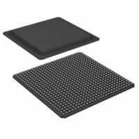
XC2V3000-4FGG676C Xilinx Inc, XC2V3000-4FGG676C Datasheet - Page 74

XC2V3000-4FGG676C
Manufacturer Part Number
XC2V3000-4FGG676C
Description
FPGA Virtex-II™ Family 3M Gates 32256 Cells 650MHz 0.15um/0.12um (CMOS) Technology 1.5V 676-Pin FBGA
Manufacturer
Xilinx Inc
Series
Virtex™-IIr
Datasheet
1.XC2V250-4FGG256C.pdf
(318 pages)
Specifications of XC2V3000-4FGG676C
Package
676FBGA
Family Name
Virtex-IIÂ
Device Logic Units
32256
Device System Gates
3000000
Number Of Registers
28672
Maximum Internal Frequency
650 MHz
Typical Operating Supply Voltage
1.5 V
Maximum Number Of User I/os
484
Ram Bits
1769472
Number Of Labs/clbs
3584
Total Ram Bits
1769472
Number Of I /o
484
Number Of Gates
3000000
Voltage - Supply
1.425 V ~ 1.575 V
Mounting Type
Surface Mount
Operating Temperature
0°C ~ 85°C
Package / Case
676-BBGA
Lead Free Status / RoHS Status
Lead free / RoHS Compliant
Number Of Logic Elements/cells
-
Lead Free Status / RoHS Status
Lead free / RoHS Compliant
Other names
122-1354
Available stocks
Company
Part Number
Manufacturer
Quantity
Price
Company:
Part Number:
XC2V3000-4FGG676C
Manufacturer:
XILINX
Quantity:
1 831
Company:
Part Number:
XC2V3000-4FGG676C
Manufacturer:
Xilinx Inc
Quantity:
10 000
- Current page: 74 of 318
- Download datasheet (3Mb)
Block SelectRAM Switching Characteristics
Table 28: Block SelectRAM Switching Characteristics
TBUF Switching Characteristics
Table 29: TBUF Switching Characteristics
DS031-3 (v3.5) November 5, 2007
Product Specification
Sequential Delays
Clock CLK to DOUT output
Setup and Hold Times Before Clock CLK
ADDR inputs
DIN inputs
EN input
RST input
WEN input
Clock CLK
CLKA to CLKB setup time for different ports
Minimum Pulse Width, High
Minimum Pulse Width, Low
Combinatorial Delays
IN input to OUT output
TRI input to OUT output high-impedance
TRI input to valid data on OUT output
R
Description
Description
T
T
T
T
T
BWCK
BACK
BDCK
BECK
BRCK
Symbol
www.xilinx.com
T
T
T
T
BPWH
BCKO
BCCS
BPWL
/T
/T
/T
/T
/T
BCKA
BCKD
BCKE
BCKR
BCKW
Virtex-II Platform FPGAs: DC and Switching Characteristics
0.95/–0.46
1.31/–0.71
0.57/–0.19
0.29/ 0.00
0.29/ 0.00
Symbol
2.10
1.17
1.17
1.0
T
T
-6
T
OFF
ON
IO
Speed Grade
1.04/–0.50
1.44/–0.78
0.63/–0.21
0.32/ 0.00
0.32/ 0.00
0.45
0.44
0.44
2.31
1.29
1.29
-6
1.0
-5
Speed Grade
0.50
0.48
0.48
-5
1.20/–0.58
1.65/–0.90
0.72/–0.25
0.36/ 0.00
0.36/ 0.00
2.65
1.48
1.48
1.0
-4
0.58
0.55
0.55
-4
Module 3 of 4
ns, Max
ns, Max
ns, Max
ns, Max
Units
ns, Min
ns, Min
ns, Min
ns, Min
ns, Min
ns, min
ns, Min
ns, Min
Units
26
Related parts for XC2V3000-4FGG676C
Image
Part Number
Description
Manufacturer
Datasheet
Request
R

Part Number:
Description:
IC VIRTEX-II FPGA 3M 676-FBGA
Manufacturer:
Xilinx Inc
Datasheet:

Part Number:
Description:
IC VIRTEX-II FPGA 3M 1152-FCBGA
Manufacturer:
Xilinx Inc
Datasheet:

Part Number:
Description:
IC FPGA VIRTEX II 3M 957-FCBGA
Manufacturer:
Xilinx Inc
Datasheet:

Part Number:
Description:
IC FPGA VIRTEX-II 3M 676-FBGA
Manufacturer:
Xilinx Inc
Datasheet:

Part Number:
Description:
IC FPGA VIRTEX II 3M 957-FCBGA
Manufacturer:
Xilinx Inc
Datasheet:

Part Number:
Description:
IC FPGA VIRTEX-II 3M 1152-FBGA
Manufacturer:
Xilinx Inc
Datasheet:

Part Number:
Description:
IC FPGA VIRTEX-II 3M 1152-FBGA
Manufacturer:
Xilinx Inc
Datasheet:

Part Number:
Description:
IC FPGA VIRTEX-II 3M 676-FBGA
Manufacturer:
Xilinx Inc
Datasheet:

Part Number:
Description:
IC FPGA VIRTEX-II 3M 676-FBGA
Manufacturer:
Xilinx Inc
Datasheet:

Part Number:
Description:
IC FPGA VIRTEX-II 3M 1152-FBGA
Manufacturer:
Xilinx Inc
Datasheet:

Part Number:
Description:
IC FPGA VIRTEX-II 3M 1152-FBGA
Manufacturer:
Xilinx Inc
Datasheet:

Part Number:
Description:
IC FPGA VIRTEX-II 676FGBGA
Manufacturer:
Xilinx Inc
Datasheet:

Part Number:
Description:
IC FPGA VIRTEX-II 728PBGA
Manufacturer:
Xilinx Inc
Datasheet:

Part Number:
Description:
IC FPGA VIRTEX-II 1152FCBGA
Manufacturer:
Xilinx Inc
Datasheet:

Part Number:
Description:
IC FPGA VIRTEX-II 957FCBGA
Manufacturer:
Xilinx Inc
Datasheet:


