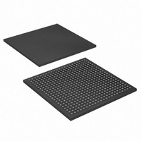
XC3SD3400A-4CSG484C Xilinx Inc, XC3SD3400A-4CSG484C Datasheet - Page 54

XC3SD3400A-4CSG484C
Manufacturer Part Number
XC3SD3400A-4CSG484C
Description
FPGA Spartan®-3A Family 3.4M Gates 53712 Cells 667MHz 90nm Technology 1.2V 484-Pin LCSBGA
Manufacturer
Xilinx Inc
Series
Spartan™-3A DSPr
Datasheets
1.XC3S50A-4VQG100C.pdf
(7 pages)
2.XC3SD3400A-4FGG676C.pdf
(4 pages)
3.XC3SD3400A-4FGG676C.pdf
(101 pages)
Specifications of XC3SD3400A-4CSG484C
Package
484LCSBGA
Family Name
Spartan®-3A
Device Logic Units
53712
Device System Gates
3400000
Maximum Internal Frequency
667 MHz
Typical Operating Supply Voltage
1.2 V
Maximum Number Of User I/os
309
Ram Bits
2322432
Number Of Logic Elements/cells
53712
Number Of Labs/clbs
5968
Total Ram Bits
2322432
Number Of I /o
309
Number Of Gates
3400000
Voltage - Supply
1.14 V ~ 1.26 V
Mounting Type
Surface Mount
Operating Temperature
0°C ~ 85°C
Package / Case
484-FBGA, CSPBGA
Lead Free Status / RoHS Status
Lead free / RoHS Compliant
For Use With
122-1532 - KIT DEVELOPMENT SPARTAN 3ADSP
Lead Free Status / RoHS Status
Lead free / RoHS Compliant
Other names
122-1540
Available stocks
Company
Part Number
Manufacturer
Quantity
Price
Company:
Part Number:
XC3SD3400A-4CSG484C
Manufacturer:
XILINX
Quantity:
177
Company:
Part Number:
XC3SD3400A-4CSG484C
Manufacturer:
XILINX
Quantity:
110
Part Number:
XC3SD3400A-4CSG484C
Manufacturer:
XILINX/赛灵思
Quantity:
20 000
Company:
Part Number:
XC3SD3400A-4CSG484CL
Manufacturer:
XILINX
Quantity:
123
Master Serial and Slave Serial Mode Timing
X-Ref Target - Figure 11
Table 50: Timing for the Master Serial and Slave Serial Configuration Modes
DS610 (v3.0) October 4, 2010
Product Specification
Notes:
1.
2.
(Input/Output)
Clock-to-Output Times
T
Setup Times
T
Hold Times
T
Clock Timing
T
T
F
(Open-Drain)
CCO
DCC
CCD
CCH
CCL
CCSER
Symbol
PROG_B
The numbers in this table are based on the operating conditions set forth in
For serial configuration with a daisy-chain of multiple FPGAs, the maximum limit is 25 MHz.
(Output)
INIT_B
(Input)
(Input)
CCLK
DOUT
DIN
The time from the falling transition on the CCLK pin to data appearing at the
DOUT pin
The time from the setup of data at the DIN pin to the rising transition at the
CCLK pin
The time from the rising transition at the CCLK pin to the point when data is
last held at the DIN pin
High pulse width at the CCLK input pin
Low pulse width at the CCLK input pin
Frequency of the clock signal at the
CCLK input pin
Figure 11: Waveforms for Master Serial and Slave Serial Configuration
(2)
Description
T
DCC
Bit 0
No bitstream compression
With bitstream compression
Spartan-3A DSP FPGA Family: DC and Switching Characteristics
www.xilinx.com
T
CCD
Bit 1
Table
7.
T
T
Master
Master
Master
Master
Slave/
MCCL
SCCL
Slave
Slave
Slave
Slave
Both
Both
Bit n
1/F
CCSER
T
CCO
Bit n-64
Bit n+1
All Speed Grades
Min
1.5
0.0
1.0
T
7
0
0
T
SCCH
MCCH
See
See
See
See
Bit n-63
Table 48
Table 49
Table 48
Table 49
Max
100
100
10
–
–
–
DS312-3_05_103105
Units
MHz
MHz
ns
ns
ns
ns
54


