TR7001 RFM, TR7001 Datasheet - Page 7

TR7001
Manufacturer Part Number
TR7001
Description
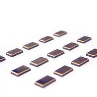
RF Transceiver 3G ASH Transceiver 315 MHz 115.2 kbps
Manufacturer
RFM
Datasheet
1.TR7001.pdf
(15 pages)
Specifications of TR7001
Wireless Frequency
315 MHz
Output Power
10 mW
Mounting Style
SMD/SMT
Package / Case
SM3-20H
Modulation
OOK/ASK
Lead Free Status / RoHS Status
Lead free / RoHS Compliant
CFG0 Bit 6 - When this bit is 0, the radio is in the receive mode (provided
CFG0 Bit 7 is 0). When this bit is 1, the radio is in one of the transmit
modes. Note the radio will transmit using OOK or ASK modulation,
depending on the value of CFG0 Bit 5. The power-on default value of this
bit is 0.
CFG0 Bit 5 - When this bit is 0, the transmitter uses OOK modulation.
When this bit is 1, the transmitter uses ASK modulation. The power-on
default value of this bit is 0.
CFG0 Bit 4 - This bit should always be set to 0 in the TR7001. The power-
on default value of this bit is 0.
CFG0 Bits 3, 2 - The states of these two bits set the basic operating mode
of the radio as shown below. The power-on default value of these two
bits is 0.
CFG0 Bit 1 - This bit should always be set to 0 in the TR7001. The power-
on default value of this bit is 0.
CFG0 Bit 0 - Setting this bit to logic 1 enables the internal start symbol
(vector) detection and the data and clock recovery circuit. When active,
this function continuously tests for a 16-bit start symbol, 0xE2E2 (hex).
Data clocking begins in the middle of the first bit following the 16-bit start
symbol, and clocking continues until CFG0 Bit 0 is reset to a logic 0. Note
that CFG0 Bit 0 must be set to back to a logic 1 to re-enable the start sym-
bol detection and the data and clock recovery circuit. The common way to
use this function is for the host processor to set this bit to a 1 when it is
ready to receive a message. When a start symbol is detected, data clock-
ing begins, and the host processor inputs the message bits. Once all of
the bits in the message are received, the host processor resets this bit to 0
to end data clocking. After the current message has been processed, the
host processor sets this bit to 1 again to enable detection of the next mes-
sage. The power-on default value of this bit is 0.
The start symbol pattern is sent starting with the MSB. This start symbol
pattern will not occur in a message that has been encoded for DC-balance
using either Manchester encoding or 8-to-12 bit symbolization using the
encoding table given below. Note that the table is given for 4-to-6 bit
encoding, so each byte of the message is encoded starting with the high
nibble and then the low nibble.
RF Monolithics, Inc.
RFM Europe
©1999 by RF Monolithics, Inc. The stylized RFM logo are registered trademarks of RF Monolithics, Inc.
Adress
Bit 3
0
1
2
0
0
1
1
LoSyn
Name
CFG0
CFG1
Bit 2
Phone: (972) 233-2903
Phone: 44 1963 251383
0
1
0
1
Sleep
Bit 7
Test
-
Single-channel Mode
VCOlock
LOSyn6
TX/RX
Not Used
Not Used
Not Used
Bit 6
Mode
ASK/OOK
LOSyn5
Fax: (972) 387-8148
Fax: 44 1963 251510
Bit 5
-
Figure 3
LOSyn4
Bit 4
CFG1 Bit 7 - This bit is unused in the TR7001.
CFG1 Bit 6 - This bit is a Read Only bit. Writing has no effect. When per-
forming a read and this bit is set, this indicates that the internal VCO is
locked and ready to transmit or receive data.
CFG1 Bit 5 - This bit is unused in the TR7001.
CFG1 Bit 4 - This bit is unused in the TR7001.
CFG1 Bits 3, 2, 1, 0 - These bits select the internal data and clock recov-
ery data (bit) rate as shown in the table below. The power-on default value
of these bits is 0.
LOSyn Bit 7 - This bit is only used in product testing. It should always be
set to 0 for normal operation. The power-on default value of this bit is 0.
LOSyn Bits 6, 5, 4, 3, 2, 1, 0 -These bits have no function in the TR7001
and can be written as either a logic 1 or a logic 0.
Note that data to/from the configuration registers is clocked in/out MSB
first. See the Control Register Read/Write Detail and Control Register
Read/Write Timing Drawings for additional details.
-
-
Nibble Hex Value
LOSyn3
Mode 1
Bit 3
BR3
C
D
0
1
2
3
4
5
6
7
8
9
A
B
E
F
LOSyn2
Mode 0
Bit 2
BR2
E-mail: info@rfm.com
http://www.rfm.com
TR7001-11062007
Symbol Hex Value (6 bits)
LOSyn1
Bit 1
BR1
-
0D
0E
1A
1C
2A
2C
13
15
16
19
23
25
26
29
32
34
LOSyn0
Page 7 of 15
SV En
Bit 0
BR0


