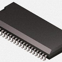
U4091BM-RFNY19 Atmel, U4091BM-RFNY19 Datasheet - Page 24

U4091BM-RFNY19
Manufacturer Part Number
U4091BM-RFNY19
Description
RF Wireless Misc COM.CORDED - FEATURE PHONE CIRCUIT
Manufacturer
Atmel
Type
Programmable Telephone Audio Processorr
Datasheet
1.U4091BM-RFNG3Y_19.pdf
(40 pages)
Specifications of U4091BM-RFNY19
Operating Frequency
100 KHz
Operating Temperature Range
- 55 C to +150 C
Package / Case
SSO-44
Mounting Style
SMD/SMT
13. Analog-to-Digital Converter (ADC)
24
Atmel U4091BM-R
This circuit is a 7-bit successive-approximation analog-to-digital converter in switched capaci-
tor technique. An internal band gap circuit generates a 1.25-V reference voltage which is the
equivalent of 1 MSB (1 LSB = 19.5mV). The possible input voltage at ADIN is 0V to 2.48V.
The ADC needs an SOC (Start Of Conversion) signal. In the High phase of the SOC signal,
the ADC is reset. Then, 50µs after the beginning of the Low phase of the SOC signal, the ADC
generates an EOC (End Of Conversion) signal which indicates that the conversion is finished.
The rising edge of EOC generates an interrupt at the INT output. The result can be read out by
the serial bus.
Voltages higher than 2.45V have to be divided. The signal connected to the ADC is deter-
mined by 4 bits: ADC0, ADC1, ADC2 and ADC3. TLDR/TLDT measuring is possible relative to
a preceding reference measurement. The current range of IL can be doubled by ADCR. If
ADCR is High, S has the value 0.5, otherwise S = 1.
The source impedance at ADIN must be lower than 250kΩ.
Accuracy: 1 LSB + 3%
Figure 13-1. Timing of ADC
Figure 13-2. ADC Input Selection
IL x 20mV/(1 mA x S )
EOC
SOC
8 x (TLDR - REF)
8 x (TLDT - REF)
0.4 x VMP S
0.4 x S AO1
0.4 x OFF1
0.4 x OFF2
0.4 x OFF3
0.4 x VMP
0.4 x VB
ADIN
50µs
ADC
S OC
EOC
MS B
BIT5
BIT4
BIT3
BIT2
BIT1
LS B
4872B–CORD–01/11


