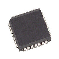
CY7B923-JCT Cypress Semiconductor Corp, CY7B923-JCT Datasheet - Page 13

CY7B923-JCT
Manufacturer Part Number
CY7B923-JCT
Description
Manufacturer
Cypress Semiconductor Corp
Datasheet
1.CY7B923-JCT.pdf
(40 pages)
Specifications of CY7B923-JCT
Lead Free Status / RoHS Status
Not Compliant
Bypass Mode Operation
In the bypass mode, the input data is interpreted as 10 bits
(D
data to be serialized and sent over the link. This data can use
any encoding method suitable to the designer. The only restric-
tions upon the data encoding method is that it contain suitable
transition density for the receiver PLL data synchronizer (one per
10-bit byte), and that it be compatible with the transmission
media.
Data loaded into the Input register on the rising edge of CKW is
loaded into the shifter on the subsequent rising edges of CKW.
It will then be shifted to the outputs one bit at a time using the
internal clock generated by the clock generator. The first bit of
the transmission character (D
OUTB±, and OUTC±) after the next CKW edge.
While in either the encoded mode or bypass mode, if a CKW
edge arrives when the inputs are not enabled (ENA and ENN
both HIGH), the encoder inserts a pad character K28.5 (for
example, C5.0) to maintain proper link synchronization (in the
bypass mode the proper sense of running disparity cannot be
guaranteed for the first pad character, but is correct for all pad
characters that follow). This automatic insertion of pad
characters can be inhibited by insuring that the transmitter is
always enabled (that is, ENA or ENN is hard-wired LOW).
PECL Output Functional and Connection Options
The three pairs of PECL outputs all contain the same information
and are intended for use in systems with multiple connections.
Each output pair may be connected to a different serial media,
each of which may be a different length, link type, or interface
technology. For systems that do not require all three output pairs,
the unused pairs should be wired to V
dissipated by the output circuit, and to minimize unwanted noise
generation. An internal voltage comparator detects when an
output differential pair is wired to V
for that pair to be disabled. This results in a power savings of
around 5 mA for each unused pair.
Document #: 38-02017 Rev. *H
b–h
), SC/D (D
a
), and SVS (D
a
) appears at the output (OUTA±,
j
) of pre-encoded transmission
CC
, causing the current source
CC
to minimize the power
In systems that require the outputs to be shut off during some
periods when link transmission is prohibited (for example, for
laser safety functions), the FOTO input can be asserted. While it
is possible to insure that the output state of the PECL drivers is
LOW (that is, light is off) by sending all 0s in bypass mode, it is
often inconvenient to insert this level of control into the data
transmission channel, and it is impossible in encoded mode.
FOTO is provided to simplify and augment this control function
(typically found in laser-based transmission systems). FOTO will
force OUTA+ and OUTB+ to go LOW, OUTA– and OUTB– to go
HIGH, while allowing OUTC± to continue to function normally
(OUTC is typically used as a diagnostic feedback and cannot be
disabled). This separation of function allows various system
configurations without undue load on the control function or data
channel logic.
Transmitter Serial Data Characteristics
The CY7B923 HOTLink transmitter serial output conforms to the
requirements of the Fibre Channel specification. The serial data
output is controlled by an internal PLL that multiplies the
frequency of CKW by 10 to maintain the proper bit clock
frequency. The jitter characteristics (including both PLL and logic
components) are as follows:
■
■
Transmitter Test Mode Description
The CY7B923 transmitter offers two types of test mode
operation, BIST mode and Test mode. In a normal system appli-
cation, the BIST mode can be used to check the functionality of
the transmitter, the receiver, and the link connecting them. This
mode is available with minimal impact on user system logic, and
can be used as part of the normal system diagnostics. Typical
connections and timing are shown in
Deterministic Jitter (D
measured while sending a continuous K28.5 (C5.0).
Random Jitter (R
while sending a continuous K28.7 (C7.0).
j
) < 175 ps (peak-peak). Typically measured
j
) < 35 ps (peak-peak). Typically
CY7B923, CY7B933
Figure 8 on page
Page 13 of 40
15.
[+] Feedback


