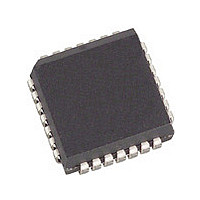
CY7B923-JCT Cypress Semiconductor Corp, CY7B923-JCT Datasheet - Page 8

CY7B923-JCT
Manufacturer Part Number
CY7B923-JCT
Description
Manufacturer
Cypress Semiconductor Corp
Datasheet
1.CY7B923-JCT.pdf
(40 pages)
Specifications of CY7B923-JCT
Lead Free Status / RoHS Status
Not Compliant
Table 2. CY7B933 HOTLink Receiver (continued)
CY7B923 HOTLink Transmitter Block
Diagram Description
Input Register
The input register holds the data to be processed by the HOTLink
transmitter and allows the input timing to be made consistent with
standard FIFOs. The input register is clocked by CKW and
loaded with information on the D
enable inputs (ENA and ENN) allow the user to choose when
data is loaded in the register. Asserting Enable, active LOW
(ENA) causes the inputs to be loaded in the register on the rising
edge of CKW. If ENN (Enable Next, active LOW) is asserted
when CKW rises, the data present on the inputs on the next rising
edge of CKW are loaded into the Input register. If neither ENA
nor ENN are asserted LOW on the rising edge of CKW, then a
SYNC (K28.5) character is sent. These two inputs allow proper
timing and function for compatibility with either asynchronous
FIFOs or clocked FIFOs without external logic, as shown in
Figure
In BIST mode, the input register becomes the signature pattern
generator by logically converting the parallel input register into a
linear feedback shift register (LFSR). When enabled, this LFSR
generates a 511-byte sequence that includes all data and special
character codes, including the explicit violation symbols. This
pattern provides a predictable but pseudo-random sequence that
can be matched to an identical LFSR in the receiver.
Encoder
The encoder transforms the input data held by the input register
into a form more suitable for transmission on a serial interface
link. The code used is specified by ANSI X3.230 (Fibre Channel)
and the IBM ESCON channel (see the table
Characters (SC/D = LOW) on page
inputs are converted to either a data symbol or a special
character, depending upon the state of the SC/D input. If SC/D
is HIGH, the data inputs represent a control code and are
encoded using the special character code table. If SC/D is LOW,
the data inputs are converted using the data code table. If a byte
time passes with the inputs disabled, the encoder outputs a
special character comma K28.5 (or SYNC) that maintains link
synchronization. SVS input forces the transmission of a specified
violation symbol to allow the user to check the error handling
system logic in the controller or for proprietary applications.
The 8B/10B coding function of the encoder can be bypassed for
systems that include an external coder or scrambler function as
part of the controller. This bypass is controlled by setting the
MODE select pin HIGH. When in bypass mode, D
Document #: 38-02017 Rev. *H
BISTEN
V
V
GND
Name
CCN
CCQ
6.
TTL In
I/O
Built-in self-test enable. When BISTEN is LOW the Receiver awaits a D0.0 (sent once per BIST loop)
character and begins a continuous test sequence that tests the functionality of the Transmitter, the
Receiver, and the link connecting them. In BIST mode the status of the test can be monitored with RDY
and RVS outputs. In normal use BISTEN is held HIGH or wired to V
Q
Power for output drivers.
Power for internal circuitry.
Ground.
Description
0–7
0-7
.
, SC/D, and SVS pins. Two
21). The eight D
Valid Data
a-j
0–7
(note that
data
the bit order is specified in the fibre channel 8B/10B code)
become the ten inputs to the shifter, with D
be shifted out.
Shifter
The shifter accepts parallel data from the encoder after each byte
time and shifts it to the serial interface output buffers using a PLL
multiplied bit clock that runs at 10 times the byte clock rate.
Timing for the parallel transfer is controlled by the counter
included in the clock generator and is not affected by signal
levels or timing at the input pins.
OutA, OutB, OutC
The serial interface PECL output buffers (ECL100K referenced
to +5 V) are the drivers for the serial media. They are all
connected to the shifter and contain the same serial data. Two of
the output pairs (OUTA± and OUTB±) are controllable by the
FOTO input and can be disabled by the system controller to force
a logical zero (that is, “light off”) at the outputs. The third output
pair (OUTC±) is not affected by FOTO and supplies a continuous
data stream suitable for loopback testing of the subsystem.
OUTA± and OUTB± responds to FOTO input changes within a
few bit times. However, since FOTO is not synchronized with the
transmitter data stream, the outputs will be forced off or turned
on at arbitrary points in a transmitted byte. This function is
intended to augment an external laser safety controller and as
an aid for Receiver PLL testing.
In wire-based systems, control of the outputs may not be
required, and FOTO can be strapped LOW. The three outputs
are intended to add system and architectural flexibility by offering
identical serial bit streams with separate interfaces for redundant
connections or for multiple destinations. Unneeded outputs can
be wired to VCC to disable and power down the unused output
circuitry.
Clock Generator
The clock generator is an embedded PLL that takes a byte-rate
reference clock (CKW) and multiplies it by 10 to create a bit rate
clock for driving the serial shifter. The byte rate reference comes
from CKW, the rising edge of which clocks data into the input
register. This clock must be a crystal referenced pulse stream
that has a frequency between the minimum and maximum
specified for the HOTLink transmitter/receiver pair. Signals
controlled by this block form the bit clock and the timing signals
that control internal data transfers between the input register and
the shifter.
CC
. BISTEN has the same timing as
CY7B923, CY7B933
a
being the first bit to
Page 8 of 40
[+] Feedback


