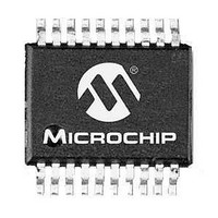
PIC16F1507-I/SO Microchip Technology, PIC16F1507-I/SO Datasheet - Page 162

PIC16F1507-I/SO
Manufacturer Part Number
PIC16F1507-I/SO
Description
3.5KB Flash, 128B RAM, 18 I/O, CLC, CWG, DDS, 10-bit ADC 20 SOIC .300in TUBE
Manufacturer
Microchip Technology
Series
PIC® 16Fr
Datasheets
1.PIC16F1507-EML.pdf
(266 pages)
2.PIC16F1507-EML.pdf
(26 pages)
3.PIC16F1507-EML.pdf
(40 pages)
Specifications of PIC16F1507-I/SO
Processor Series
PIC16
Core
PIC16F
Data Bus Width
8 bit
Program Memory Type
Flash
Program Memory Size
3.5 KB
Data Ram Size
128 B
Interface Type
ICSP
Maximum Clock Frequency
20 MHz
Number Of Programmable I/os
18
Number Of Timers
3
Operating Supply Voltage
2.3 V to 5.5 V
Maximum Operating Temperature
+ 85 C
Mounting Style
SMD/SMT
Package / Case
SOIC-20
Minimum Operating Temperature
- 40 C
Operating Temperature Range
- 40 C to + 85 C
Supply Current (max)
30 uA
Core Processor
PIC
Core Size
8-Bit
Speed
20MHz
Connectivity
-
Peripherals
Brown-out Detect/Reset, POR, PWM, WDT
Number Of I /o
17
Eeprom Size
-
Ram Size
128 x 8
Voltage - Supply (vcc/vdd)
2.3 V ~ 5.5 V
Data Converters
A/D 12x10b
Oscillator Type
Internal
Operating Temperature
-40°C ~ 85°C
Lead Free Status / Rohs Status
Details
Available stocks
Company
Part Number
Manufacturer
Quantity
Price
Part Number:
PIC16F1507-I/SO
Manufacturer:
MICROCHI
Quantity:
20 000
- Current page: 162 of 266
- Download datasheet (3Mb)
20.1
Programming the CLCx module is performed by config-
uring the 4 stages in the logic signal flow. The 4 stages
are:
• Data selection
• Data gating
• Logic function selection
• Output polarity
Each stage is setup at run time by writing to the corre-
sponding CLCx Special Function Registers. This has
the added advantage of permitting logic reconfiguration
on-the-fly during program execution.
TABLE 20-1:
2011 Microchip Technology Inc.
CLCxIN[0]
CLCxIN[1]
CLCxIN[2]
CLCxIN[3]
CLCxIN[4]
CLCxIN[5]
CLCxIN[6]
CLCxIN[7]
CLCxIN[8]
CLCxIN[9]
CLCxIN[10]
CLCxIN[11]
CLCxIN[12]
CLCxIN[13]
CLCxIN[14]
CLCxIN[15]
Data Input
CLCx Setup
CLCx DATA INPUT SELECTION
lcxd1
D1S
000
001
010
011
100
101
110
111
—
—
—
—
—
—
—
—
lcxd2
D2S
000
001
010
011
100
101
110
111
—
—
—
—
—
—
—
—
lcxd3
D3S
000
001
010
011
100
101
110
111
Preliminary
—
—
—
—
—
—
—
—
lcxd4
20.1.1
There are 16 signals available as inputs to the configu-
rable logic. Four 8-input multiplexers are used to select
the inputs to pass on to the next stage. The 16 inputs to
the multiplexers are arranged in groups of four. Each
group is available to two of the four multiplexers, in
each case, paired with a different group. This arrange-
ment makes possible selection of up to two from a
group without precluding a selection from another
group.
Data inputs are selected with the CLCxSEL0 and
CLCxSEL1 registers
respectively).
Data inputs are selected with CLCxSEL0 and
CLCxSEL1 registers
respectively).
Data selection is through four multiplexers as indicated
on the left side of
are identified by a generic numbered input name.
Table 20-1
actual signal for each CLC module. The columns labeled
lcxd1 through lcxd4 indicate the MUX output for the
selected data input. D1S through D4S are abbreviations
for the MUX select input codes: LCxD1S<2:0> through
LCxD4S<2:0>, respectively. Selecting a data input in a
column excludes all other inputs in that column.
D4S
100
101
110
111
000
001
010
011
—
—
—
—
—
—
—
—
Note:
CLC1IN0
CLC1IN1
Reserved
Reserved
F
TMR0IF
TMR1IF
TMR2 = PR2
lcx1_out
lcx2_out
lcx3_out
lcx4_out
NCO1OUT
HFINTOSC
PWM3OUT
PWM4OUT
OSC
correlates the generic input name to the
DATA SELECTION
Data selections are undefined at power-up.
PIC16(L)F1507
CLC 1
Figure
(Register 20-3
(Register 20-3
20-2. Data inputs in the figure
CLC2IN0
CLC2IN1
Reserved
Reserved
F
TMR0IF
TMR1IF
TMR2 = PR2
lcx1_out
lcx2_out
lcx3_out
lcx4_out
ADCFRC
PWM1OUT
PWM2OUT
LFINTOSC
OSC
DS41586A-page 162
and
and
CLC 2
Register
Register
20-4,
20-4,
Related parts for PIC16F1507-I/SO
Image
Part Number
Description
Manufacturer
Datasheet
Request
R

Part Number:
Description:
IC, 8BIT MCU, PIC16F, 32MHZ, SOIC-18
Manufacturer:
Microchip Technology
Datasheet:

Part Number:
Description:
IC, 8BIT MCU, PIC16F, 32MHZ, SSOP-20
Manufacturer:
Microchip Technology
Datasheet:

Part Number:
Description:
IC, 8BIT MCU, PIC16F, 32MHZ, DIP-18
Manufacturer:
Microchip Technology
Datasheet:

Part Number:
Description:
IC, 8BIT MCU, PIC16F, 32MHZ, QFN-28
Manufacturer:
Microchip Technology
Datasheet:

Part Number:
Description:
IC, 8BIT MCU, PIC16F, 32MHZ, QFN-28
Manufacturer:
Microchip Technology
Datasheet:

Part Number:
Description:
IC, 8BIT MCU, PIC16F, 32MHZ, QFN-28
Manufacturer:
Microchip Technology
Datasheet:

Part Number:
Description:
IC, 8BIT MCU, PIC16F, 32MHZ, SSOP-20
Manufacturer:
Microchip Technology
Datasheet:

Part Number:
Description:
IC, 8BIT MCU, PIC16F, 20MHZ, DIP-40
Manufacturer:
Microchip Technology
Datasheet:

Part Number:
Description:
IC, 8BIT MCU, PIC16F, 32MHZ, QFN-28
Manufacturer:
Microchip Technology
Datasheet:

Part Number:
Description:
IC, 8BIT MCU, PIC16F, 20MHZ, MQFP-44
Manufacturer:
Microchip Technology
Datasheet:

Part Number:
Description:
IC, 8BIT MCU, PIC16F, 20MHZ, QFN-20
Manufacturer:
Microchip Technology
Datasheet:

Part Number:
Description:
IC, 8BIT MCU, PIC16F, 32MHZ, QFN-28
Manufacturer:
Microchip Technology
Datasheet:

Part Number:
Description:
MCU 14KB FLASH 768B RAM 64-TQFP
Manufacturer:
Microchip Technology
Datasheet:

Part Number:
Description:
7 KB Flash, 384 Bytes RAM, 32 MHz Int. Osc, 16 I/0, Enhanced Mid Range Core, Low
Manufacturer:
Microchip Technology

Part Number:
Description:
14KB Flash, 512B RAM, 256B EEPROM, LCD, 1.8-5.5V 40 UQFN 5x5x0.5mm TUBE
Manufacturer:
Microchip Technology
Datasheet:


