PIC16F1507-I/SS Microchip Technology, PIC16F1507-I/SS Datasheet - Page 67
PIC16F1507-I/SS
Manufacturer Part Number
PIC16F1507-I/SS
Description
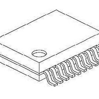
3.5KB Flash, 128B RAM, 18 I/O, CLC, CWG, DDS, 10-bit ADC 20 SSOP .209in TUBE
Manufacturer
Microchip Technology
Series
PIC® 16Fr
Datasheets
1.PIC16F1507-EML.pdf
(266 pages)
2.PIC16F1507-EML.pdf
(26 pages)
3.PIC16F1507-EML.pdf
(40 pages)
Specifications of PIC16F1507-I/SS
Processor Series
PIC16
Core
PIC16F
Data Bus Width
8 bit
Program Memory Type
Flash
Program Memory Size
3.5 KB
Data Ram Size
128 B
Interface Type
ICSP
Maximum Clock Frequency
20 MHz
Number Of Programmable I/os
18
Number Of Timers
3
Operating Supply Voltage
2.3 V to 5.5 V
Maximum Operating Temperature
+ 85 C
Mounting Style
SMD/SMT
Package / Case
SSOP-20
Minimum Operating Temperature
- 40 C
Operating Temperature Range
- 40 C to + 85 C
Supply Current (max)
30 uA
Core Processor
PIC
Core Size
8-Bit
Speed
20MHz
Connectivity
-
Peripherals
Brown-out Detect/Reset, POR, PWM, WDT
Number Of I /o
17
Eeprom Size
-
Ram Size
128 x 8
Voltage - Supply (vcc/vdd)
2.3 V ~ 5.5 V
Data Converters
A/D 12x10b
Oscillator Type
Internal
Operating Temperature
-40°C ~ 85°C
Lead Free Status / Rohs Status
Details
Available stocks
Company
Part Number
Manufacturer
Quantity
Price
Company:

Part Number:
PIC16F1507-I/SS
Manufacturer:
MICROCHIP
Quantity:
5 000
Part Number:
PIC16F1507-I/SS
Manufacturer:
MICROCHIP/微芯
Quantity:
20 000


PIC16(L)F1507
7.6.2
The PIE1 register contains the interrupt enable bits, as
shown in
REGISTER 7-2:
DS41586A-page 67
bit 7
Legend:
R = Readable bit
u = Bit is unchanged
‘1’ = Bit is set
bit 7
bit 6
bit 5-2
bit 1
bit 0
TMR1GIE
R/W-0/0
Register
PIE1 REGISTER
TMR1GIE: Timer1 Gate Interrupt Enable bit
1 = Enables the Timer1 Gate Acquisition interrupt
0 = Disables the Timer1 Gate Acquisition interrupt
ADIE: A/D Converter (ADC) Interrupt Enable bit
1 = Enables the ADC interrupt
0 = Disables the ADC interrupt
Unimplemented: Read as ‘0’
TMR2IE: TMR2 to PR2 Match Interrupt Enable bit
1 = Enables the Timer2 to PR2 match interrupt
0 = Disables the Timer2 to PR2 match interrupt
TMR1IE: Timer1 Overflow Interrupt Enable bit
1 = Enables the Timer1 overflow interrupt
0 = Disables the Timer1 overflow interrupt
7-2.
R/W-0/0
ADIE
PIE1: PERIPHERAL INTERRUPT ENABLE REGISTER 1
W = Writable bit
x = Bit is unknown
‘0’ = Bit is cleared
U-0
—
U-0
Preliminary
—
U = Unimplemented bit, read as ‘0’
-n/n = Value at POR and BOR/Value at all other Resets
U-0
—
Note:
Bit PEIE of the INTCON register must be
set to enable any peripheral interrupt.
U-0
—
2011 Microchip Technology Inc.
R/W-0/0
TMR2IE
R/W-0/0
TMR1IE
bit 0
Related parts for PIC16F1507-I/SS
Image
Part Number
Description
Manufacturer
Datasheet
Request
R

Part Number:
Description:
IC, 8BIT MCU, PIC16F, 32MHZ, SOIC-18
Manufacturer:
Microchip Technology
Datasheet:

Part Number:
Description:
IC, 8BIT MCU, PIC16F, 32MHZ, SSOP-20
Manufacturer:
Microchip Technology
Datasheet:

Part Number:
Description:
IC, 8BIT MCU, PIC16F, 32MHZ, DIP-18
Manufacturer:
Microchip Technology
Datasheet:

Part Number:
Description:
IC, 8BIT MCU, PIC16F, 32MHZ, QFN-28
Manufacturer:
Microchip Technology
Datasheet:

Part Number:
Description:
IC, 8BIT MCU, PIC16F, 32MHZ, QFN-28
Manufacturer:
Microchip Technology
Datasheet:
Part Number:
Description:
IC, 8BIT MCU, PIC16F, 32MHZ, QFN-28
Manufacturer:
Microchip Technology
Datasheet:
Part Number:
Description:
IC, 8BIT MCU, PIC16F, 32MHZ, SSOP-20
Manufacturer:
Microchip Technology
Datasheet:

Part Number:
Description:
IC, 8BIT MCU, PIC16F, 20MHZ, DIP-40
Manufacturer:
Microchip Technology
Datasheet:

Part Number:
Description:
IC, 8BIT MCU, PIC16F, 32MHZ, QFN-28
Manufacturer:
Microchip Technology
Datasheet:

Part Number:
Description:
IC, 8BIT MCU, PIC16F, 20MHZ, MQFP-44
Manufacturer:
Microchip Technology
Datasheet:

Part Number:
Description:
IC, 8BIT MCU, PIC16F, 20MHZ, QFN-20
Manufacturer:
Microchip Technology
Datasheet:
Part Number:
Description:
IC, 8BIT MCU, PIC16F, 32MHZ, QFN-28
Manufacturer:
Microchip Technology
Datasheet:

Part Number:
Description:
MCU 14KB FLASH 768B RAM 64-TQFP
Manufacturer:
Microchip Technology
Datasheet:
Part Number:
Description:
7 KB Flash, 384 Bytes RAM, 32 MHz Int. Osc, 16 I/0, Enhanced Mid Range Core, Low
Manufacturer:
Microchip Technology

Part Number:
Description:
14KB Flash, 512B RAM, 256B EEPROM, LCD, 1.8-5.5V 40 UQFN 5x5x0.5mm TUBE
Manufacturer:
Microchip Technology
Datasheet: