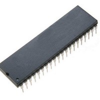
PIC16F1519-E/P Microchip Technology, PIC16F1519-E/P Datasheet - Page 297

PIC16F1519-E/P
Manufacturer Part Number
PIC16F1519-E/P
Description
40-pin, 28KB Flash, 1024B RAM, 10-bit ADC, 2xCCP, SPI, MI2C, EUSART, 2.3V-5.5V 4
Manufacturer
Microchip Technology
Series
PIC® XLP™ 16Fr
Datasheet
1.PIC16F1516-EMV.pdf
(344 pages)
Specifications of PIC16F1519-E/P
Processor Series
PIC16F151x
Core
PIC
Data Bus Width
8 bit
Program Memory Type
Flash
Program Memory Size
16 KB
Data Ram Size
1 KB
Interface Type
I2C, SPI, USART
Maximum Clock Frequency
20 MHz
Number Of Programmable I/os
36
Number Of Timers
3
Operating Supply Voltage
2.3 V to 5.5 V
Maximum Operating Temperature
+ 125 C
Mounting Style
Through Hole
Package / Case
PDIP-40
Core Processor
PIC
Core Size
8-Bit
Speed
20MHz
Connectivity
I²C, LIN, SPI, UART/USART
Peripherals
Brown-out Detect/Reset, POR, PWM, WDT
Number Of I /o
36
Eeprom Size
-
Ram Size
1K x 8
Voltage - Supply (vcc/vdd)
2.3 V ~ 5.5 V
Data Converters
A/D 28x10b
Oscillator Type
Internal
Operating Temperature
-40°C ~ 125°C
Lead Free Status / Rohs Status
Details
Available stocks
Company
Part Number
Manufacturer
Quantity
Price
Company:
Part Number:
PIC16F1519-E/PT
Manufacturer:
Microchip Technology
Quantity:
10 000
- Current page: 297 of 344
- Download datasheet (3Mb)
TABLE 25-2:
FIGURE 25-6:
2011 Microchip Technology Inc.
Standard Operating Conditions (unless otherwise stated)
Operating Temperature
OS08
OS09
OS10*
Note 1: Instruction cycle period (T
Param
No.
CLKOUT
I/O pin
(Output)
I/O pin
(Input)
*
†
2: To ensure these oscillator frequency tolerances, V
3: By design.
Cycle
F
OSC
HF
LF
T
These parameters are characterized but not tested.
Data in “Typ” column is at 3.0V, 25°C unless otherwise stated. These parameters are for design guidance only and are not
tested.
characterization data for that particular oscillator type under standard operating conditions with the device executing code.
Exceeding these specified limits may result in an unstable oscillator operation and/or higher than expected current con-
sumption. All devices are tested to operate at “min” values with an external clock applied to the OSC1 pin. When an exter-
nal clock input is used, the “max” cycle time limit is “DC” (no clock) for all devices.
possible. 0.1 F and 0.01 F values in parallel are recommended.
IOSC ST
Sym.
OSC
OSC
OSCILLATOR PARAMETERS
Internal Calibrated HFINTOSC
Frequency
Internal LFINTOSC Frequency
HFINTOSC
Wake-up from Sleep Start-up Time
Old Value
CLKOUT AND I/O TIMING
Write
-40°C T
Q4
Characteristic
(2)
CY
A
+125°C
) equals four times the input oscillator time base period. All specified values are based on
OS15
OS11
OS19
Fetch
Q1
Preliminary
OS13
Tolerance
10%
Freq.
OS18, OS19
DD
—
—
and V
SS
Min.
—
—
—
must be capacitively decoupled as close to the device as
OS17
PIC16(L)F1516/7/8/9
Typ†
16.0
31
5
OS20
OS21
OS16
Read
Q2
OS14
Max.
—
—
8
Units
MHz
kHz
s
0°C T
OS12
New Value
A
Execute
OS18
DS41452B-page 297
Conditions
+85°C
Q3
Related parts for PIC16F1519-E/P
Image
Part Number
Description
Manufacturer
Datasheet
Request
R

Part Number:
Description:
IC, 8BIT MCU, PIC16F, 32MHZ, SOIC-18
Manufacturer:
Microchip Technology
Datasheet:

Part Number:
Description:
IC, 8BIT MCU, PIC16F, 32MHZ, SSOP-20
Manufacturer:
Microchip Technology
Datasheet:

Part Number:
Description:
IC, 8BIT MCU, PIC16F, 32MHZ, DIP-18
Manufacturer:
Microchip Technology
Datasheet:

Part Number:
Description:
IC, 8BIT MCU, PIC16F, 32MHZ, QFN-28
Manufacturer:
Microchip Technology
Datasheet:

Part Number:
Description:
IC, 8BIT MCU, PIC16F, 32MHZ, QFN-28
Manufacturer:
Microchip Technology
Datasheet:

Part Number:
Description:
IC, 8BIT MCU, PIC16F, 32MHZ, QFN-28
Manufacturer:
Microchip Technology
Datasheet:

Part Number:
Description:
IC, 8BIT MCU, PIC16F, 32MHZ, SSOP-20
Manufacturer:
Microchip Technology
Datasheet:

Part Number:
Description:
IC, 8BIT MCU, PIC16F, 20MHZ, DIP-40
Manufacturer:
Microchip Technology
Datasheet:

Part Number:
Description:
IC, 8BIT MCU, PIC16F, 32MHZ, QFN-28
Manufacturer:
Microchip Technology
Datasheet:

Part Number:
Description:
IC, 8BIT MCU, PIC16F, 20MHZ, MQFP-44
Manufacturer:
Microchip Technology
Datasheet:

Part Number:
Description:
IC, 8BIT MCU, PIC16F, 20MHZ, QFN-20
Manufacturer:
Microchip Technology
Datasheet:

Part Number:
Description:
IC, 8BIT MCU, PIC16F, 32MHZ, QFN-28
Manufacturer:
Microchip Technology
Datasheet:

Part Number:
Description:
MCU 14KB FLASH 768B RAM 64-TQFP
Manufacturer:
Microchip Technology
Datasheet:

Part Number:
Description:
7 KB Flash, 384 Bytes RAM, 32 MHz Int. Osc, 16 I/0, Enhanced Mid Range Core, Low
Manufacturer:
Microchip Technology

Part Number:
Description:
14KB Flash, 512B RAM, 256B EEPROM, LCD, 1.8-5.5V 40 UQFN 5x5x0.5mm TUBE
Manufacturer:
Microchip Technology
Datasheet:


