PIC16LF1507-E/SS Microchip Technology, PIC16LF1507-E/SS Datasheet - Page 110
PIC16LF1507-E/SS
Manufacturer Part Number
PIC16LF1507-E/SS
Description
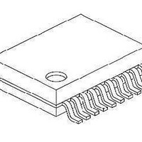
3.5KB Flash, 128B RAM, 18 I/O, CLC, CWG, DDS, 10-bit ADC 20 SSOP .209in TUBE
Manufacturer
Microchip Technology
Series
PIC® 16Fr
Datasheet
1.PIC16F1507-EML.pdf
(266 pages)
Specifications of PIC16LF1507-E/SS
Processor Series
PIC16
Core
PIC16F
Data Bus Width
8 bit
Program Memory Type
Flash
Program Memory Size
3.5 KB
Data Ram Size
128 B
Interface Type
ICSP
Maximum Clock Frequency
20 MHz
Number Of Programmable I/os
18
Number Of Timers
3
Operating Supply Voltage
2.3 V to 5.5 V
Maximum Operating Temperature
+ 125 C
Mounting Style
SMD/SMT
Package / Case
SSOP-20
Minimum Operating Temperature
- 40 C
Operating Temperature Range
- 40 C to + 125 C
Supply Current (max)
30 uA
Core Processor
PIC
Core Size
8-Bit
Speed
20MHz
Connectivity
-
Peripherals
Brown-out Detect/Reset, POR, PWM, WDT
Number Of I /o
17
Eeprom Size
-
Ram Size
128 x 8
Voltage - Supply (vcc/vdd)
1.8 V ~ 3.6 V
Data Converters
A/D 12x10b
Oscillator Type
Internal
Operating Temperature
-40°C ~ 125°C
Lead Free Status / Rohs Status
Details
Available stocks
Company
Part Number
Manufacturer
Quantity
Price

Part Number:
PIC16LF1507-E/SS
Manufacturer:
MICROCHIP/微芯
Quantity:
20 000


REGISTER 11-15: ANSELC: PORTC ANALOG SELECT REGISTER
REGISTER 11-16: WPUC: WEAK PULL-UP PORTC REGISTER
TABLE 11-8:
2011 Microchip Technology Inc.
bit 7
Legend:
R = Readable bit
u = Bit is unchanged
‘1’ = Bit is set
bit 7-6
bit 5-4
bit 3-0
Note 1:
bit 7
Legend:
R = Readable bit
u = Bit is unchanged
‘1’ = Bit is set
bit 7-0
Note 1:
ANSELC
LATC
PORTC
TRISC
WPUC
Legend:
R/W-1/1
R/W-1/1
WPUC7
ANSC7
Name
2:
When setting a pin to an analog input, the corresponding TRIS bit must be set to Input mode in order to
allow external control of the voltage on the pin.
Global WPUEN bit of the OPTION_REG register must be cleared for individual pull-ups to be enabled.
The weak pull-up device is automatically disabled if the pin is in configured as an output.
x = unknown, u = unchanged, - = unimplemented locations read as ‘0’. Shaded cells are not used by PORTC.
ANSC<7:6>: Analog Select between Analog or Digital Function on pins RC<3:0>, respectively
1 = Analog input. Pin is assigned as analog input
0 = Digital I/O. Pin is assigned to port or digital special function.
Unimplemented: Read as ‘0’
ANSC<3:0>: Analog Select between Analog or Digital Function on pins RC<3:0>, respectively
1 = Analog input. Pin is assigned as analog input
0 = Digital I/O. Pin is assigned to port or digital special function.
WPUC<7:0>: Weak Pull-Up Register bits
1 = Pull-up enabled
0 = Pull-up disabled
TRISC7
WPUC7
ANSC7
LATC7
SUMMARY OF REGISTERS ASSOCIATED WITH PORTC
R/W-1/1
Bit 7
ANSC6
R/W-1/1
WPUC6
RC7
WPUC6
TRISC6
ANSC6
LATC6
Bit 6
RC6
W = Writable bit
x = Bit is unknown
‘0’ = Bit is cleared
W = Writable bit
x = Bit is unknown
‘0’ = Bit is cleared
R/W-1/1
WPUC5
U-0
—
TRISC5
WPUC5
LATC5
Bit 5
RC5
—
R/W-1/1
WPUC4
U-0
Preliminary
—
WPUC4
TRISC4
LATC4
Bit 4
RC4
—
(1, 2)
U = Unimplemented bit, read as ‘0’
-n/n = Value at POR and BOR/Value at all other Resets
U = Unimplemented bit, read as ‘0’
-n/n = Value at POR and BOR/Value at all other Resets
R/W-1/1
WPUC3
R/W-1/1
ANSC3
TRISC3
WPUC3
ANSC3
LATC3
Bit 3
RC3
(1)
(1)
. Digital input buffer disabled.
. Digital input buffer disabled.
WPUC2
TRISC2
ANSC2
LATC2
Bit 2
R/W-1/1
WPUC2
RC2
R/W-1/1
ANSC2
PIC16(L)F1507
TRISC1
WPUC1
ANSC1
LATC1
Bit 1
RC1
R/W-1/1
R/W-1/1
ANSC1
WPUC1
WPUC0
TRISC0
ANSC0
LATC0
Bit 0
DS41586A-page 110
RC0
R/W-1/1
ANSC0
R/W-1/1
WPUC0
Register
on Page
107
106
106
106
107
bit 0
bit 0
Related parts for PIC16LF1507-E/SS
Image
Part Number
Description
Manufacturer
Datasheet
Request
R

Part Number:
Description:
IC, 8BIT MCU, PIC16LF, 32MHZ, QFN-28
Manufacturer:
Microchip Technology
Datasheet:

Part Number:
Description:
IC, 8BIT MCU, PIC16LF, 32MHZ, QFN-28
Manufacturer:
Microchip Technology
Datasheet:

Part Number:
Description:
IC, 8BIT MCU, PIC16LF, 32MHZ, DIP-18
Manufacturer:
Microchip Technology
Datasheet:

Part Number:
Description:
IC, 8BIT MCU, PIC16LF, 20MHZ, TQFP-44
Manufacturer:
Microchip Technology
Datasheet:
Part Number:
Description:
7 KB Flash, 384 Bytes RAM, 32 MHz Int. Osc, 16 I/0, Enhanced Mid Range Core, Nan
Manufacturer:
Microchip Technology

Part Number:
Description:
14KB Flash, 512B RAM, LCD, 11x10b ADC, EUSART, NanoWatt XLP 28 SOIC .300in T/R
Manufacturer:
Microchip Technology
Datasheet:
Part Number:
Description:
14KB Flash, 512B RAM, LCD, 11x10b ADC, EUSART, NanoWatt XLP 28 SSOP .209in T/R
Manufacturer:
Microchip Technology
Datasheet:
Part Number:
Description:
MCU PIC 14KB FLASH XLP 28-SSOP
Manufacturer:
Microchip Technology
Part Number:
Description:
MCU PIC 14KB FLASH XLP 28-SOIC
Manufacturer:
Microchip Technology
Part Number:
Description:
MCU PIC 512B FLASH XLP 28-UQFN
Manufacturer:
Microchip Technology
Part Number:
Description:
MCU PIC 14KB FLASH XLP 28-SPDIP
Manufacturer:
Microchip Technology

Part Number:
Description:
MCU 7KB FLASH 256B RAM 40-UQFN
Manufacturer:
Microchip Technology
Part Number:
Description:
MCU 7KB FLASH 256B RAM 44-TQFP
Manufacturer:
Microchip Technology

Part Number:
Description:
MCU 14KB FLASH 1KB RAM 28-UQFN
Manufacturer:
Microchip Technology
Part Number:
Description:
MCU PIC 14KB FLASH XLP 40-UQFN
Manufacturer:
Microchip Technology