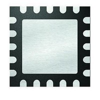
PIC18LF13K22-E/ML Microchip Technology, PIC18LF13K22-E/ML Datasheet - Page 120

PIC18LF13K22-E/ML
Manufacturer Part Number
PIC18LF13K22-E/ML
Description
8KB Flash, 256bytes RAM, 256bytes EEPROM, 16MIPS, NanoWatt XLP 20 QFN 4x4mm TUBE
Manufacturer
Microchip Technology
Series
PIC® XLP™ 18Fr
Datasheets
1.PIC18LF13K22-ISS.pdf
(388 pages)
2.PIC18LF13K22-ISS.pdf
(12 pages)
3.PIC18LF13K22-ISS.pdf
(36 pages)
Specifications of PIC18LF13K22-E/ML
Core Processor
PIC
Core Size
8-Bit
Speed
48MHz
Connectivity
I²C, LIN, SPI, UART/USART
Peripherals
Brown-out Detect/Reset, POR, PWM, WDT
Number Of I /o
17
Program Memory Size
8KB (4K x 16)
Program Memory Type
FLASH
Eeprom Size
256 x 8
Ram Size
256 x 8
Voltage - Supply (vcc/vdd)
1.8 V ~ 3.6 V
Data Converters
A/D 12x10b
Oscillator Type
Internal
Operating Temperature
-40°C ~ 125°C
Package / Case
20-VQFN Exposed Pad, 20-HVQFN, 20-SQFN, 20-DHVQFN
Processor Series
PIC18LF
Core
PIC
Data Bus Width
8 bit
Data Ram Size
256 B
Interface Type
EUSART, I2C, SPI
Maximum Clock Frequency
32 KHz
Number Of Programmable I/os
18
Number Of Timers
4
Operating Supply Voltage
1.8 V to 3.6 V
Maximum Operating Temperature
+ 125 C
Mounting Style
SMD/SMT
3rd Party Development Tools
52715-96, 52716-328, 52717-734, 52712-325, EWPIC18
Development Tools By Supplier
PG164130, DV164035, DV244005, DV164005
Minimum Operating Temperature
- 40 C
On-chip Adc
10 bit, 12 Channel
A/d Bit Size
10 bit
A/d Channels Available
12
Height
0.88 mm
Length
4 mm
Supply Voltage (max)
3.6 V
Supply Voltage (min)
1.8 V, 2.7 V
Width
4 mm
Lead Free Status / RoHS Status
Lead free / RoHS Compliant
Lead Free Status / RoHS Status
Lead free / RoHS Compliant
- Current page: 120 of 388
- Download datasheet (4Mb)
PIC18F1XK22/LF1XK22
13.4.1
In Half-Bridge mode, two pins are used as outputs to
drive push-pull loads. The PWM output signal is output
on the CCP1/P1A pin, while the complementary PWM
output signal is output on the P1B pin (see
Figure 13-6). This mode can be used for Half-Bridge
applications, as shown in Figure 13-7, or for Full-Bridge
applications, where four power switches are being
modulated with two PWM signals.
In Half-Bridge mode, the programmable dead-band delay
can be used to prevent shoot-through current in
Half-Bridge power devices. The value of the PDC<6:0>
bits of the PWM1CON register sets the number of
instruction cycles before the output is driven active. If the
value is greater than the duty cycle, the corresponding
output remains inactive during the entire cycle. See
Section 13.4.6 “Programmable Dead-Band Delay
Mode” for more details of the dead-band delay
operations.
FIGURE 13-7:
DS41365D-page 120
Standard Half-Bridge Circuit (“Push-Pull”)
Half-Bridge Output Driving a Full-Bridge Circuit
HALF-BRIDGE MODE
EXAMPLE OF HALF-BRIDGE APPLICATIONS
P1A
P1B
P1A
P1B
FET
Driver
FET
Driver
Preliminary
FET
Driver
FET
Driver
Since the P1A and P1B outputs are multiplexed with
the PORT data latches, the associated TRIS bits must
be cleared to configure P1A and P1B as outputs.
FIGURE 13-6:
P1A
P1B
td = Dead-Band Delay
Note 1: At this time, the TMR2 register is equal to the
Load
V+
(2)
(2)
2: Output signals are shown as active-high.
(1)
PR2 register.
td
Pulse Width
Load
Period
td
FET
Driver
FET
Driver
EXAMPLE OF
HALF-BRIDGE PWM
OUTPUT
2010 Microchip Technology Inc.
+
-
+
-
(1)
Period
(1)
Related parts for PIC18LF13K22-E/ML
Image
Part Number
Description
Manufacturer
Datasheet
Request
R

Part Number:
Description:
Manufacturer:
Microchip Technology Inc.
Datasheet:

Part Number:
Description:
Manufacturer:
Microchip Technology Inc.
Datasheet:

Part Number:
Description:
Manufacturer:
Microchip Technology Inc.
Datasheet:

Part Number:
Description:
Manufacturer:
Microchip Technology Inc.
Datasheet:

Part Number:
Description:
Manufacturer:
Microchip Technology Inc.
Datasheet:

Part Number:
Description:
Manufacturer:
Microchip Technology Inc.
Datasheet:

Part Number:
Description:
Manufacturer:
Microchip Technology Inc.
Datasheet:

Part Number:
Description:
Manufacturer:
Microchip Technology Inc.
Datasheet:


