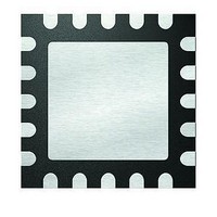
PIC18LF13K22-E/ML Microchip Technology, PIC18LF13K22-E/ML Datasheet - Page 141

PIC18LF13K22-E/ML
Manufacturer Part Number
PIC18LF13K22-E/ML
Description
8KB Flash, 256bytes RAM, 256bytes EEPROM, 16MIPS, NanoWatt XLP 20 QFN 4x4mm TUBE
Manufacturer
Microchip Technology
Series
PIC® XLP™ 18Fr
Datasheets
1.PIC18LF13K22-ISS.pdf
(388 pages)
2.PIC18LF13K22-ISS.pdf
(12 pages)
3.PIC18LF13K22-ISS.pdf
(36 pages)
Specifications of PIC18LF13K22-E/ML
Core Processor
PIC
Core Size
8-Bit
Speed
48MHz
Connectivity
I²C, LIN, SPI, UART/USART
Peripherals
Brown-out Detect/Reset, POR, PWM, WDT
Number Of I /o
17
Program Memory Size
8KB (4K x 16)
Program Memory Type
FLASH
Eeprom Size
256 x 8
Ram Size
256 x 8
Voltage - Supply (vcc/vdd)
1.8 V ~ 3.6 V
Data Converters
A/D 12x10b
Oscillator Type
Internal
Operating Temperature
-40°C ~ 125°C
Package / Case
20-VQFN Exposed Pad, 20-HVQFN, 20-SQFN, 20-DHVQFN
Processor Series
PIC18LF
Core
PIC
Data Bus Width
8 bit
Data Ram Size
256 B
Interface Type
EUSART, I2C, SPI
Maximum Clock Frequency
32 KHz
Number Of Programmable I/os
18
Number Of Timers
4
Operating Supply Voltage
1.8 V to 3.6 V
Maximum Operating Temperature
+ 125 C
Mounting Style
SMD/SMT
3rd Party Development Tools
52715-96, 52716-328, 52717-734, 52712-325, EWPIC18
Development Tools By Supplier
PG164130, DV164035, DV244005, DV164005
Minimum Operating Temperature
- 40 C
On-chip Adc
10 bit, 12 Channel
A/d Bit Size
10 bit
A/d Channels Available
12
Height
0.88 mm
Length
4 mm
Supply Voltage (max)
3.6 V
Supply Voltage (min)
1.8 V, 2.7 V
Width
4 mm
Lead Free Status / RoHS Status
Lead free / RoHS Compliant
Lead Free Status / RoHS Status
Lead free / RoHS Compliant
- Current page: 141 of 388
- Download datasheet (4Mb)
14.2.6
In Slave mode, the data is transmitted and received as
external clock pulses appear on SCK. When the last bit
is latched, the SSPIF interrupt flag bit is set.
Before enabling the module in SPI Slave mode, the clock
line must match the proper Idle state. The clock line can
be observed by reading the SCK pin. The Idle state is
determined by the CKP bit of the SSPCON1 register.
While in Slave mode, the external clock is supplied by
the external clock source on the SCK pin. This external
clock must meet the minimum high and low times as
specified in the electrical specifications.
While in Sleep mode, the slave can transmit/receive
data. When a byte is received, the device will wake-up
from Sleep.
FIGURE 14-4:
2010 Microchip Technology Inc.
SS
SCK
(CKP = 0
CKE = 0)
SCK
(CKP = 1
CKE = 0)
Write to
SSPBUF
SDO
SDI
(SMP = 0)
Input
Sample
(SMP = 0)
SSPIF
Interrupt
Flag
SSPSR to
SSPBUF
SLAVE MODE
SLAVE SYNCHRONIZATION WAVEFORM
bit 7
bit 7
bit 6
Preliminary
PIC18F1XK22/LF1XK22
14.2.7
The SS pin allows a Synchronous Slave mode. The
SPI must be in Slave mode with SS pin control enabled
(SSPCON1<3:0> = 0100). When the SS pin is low,
transmission and reception are enabled and the SDO
pin is driven. When the SS pin goes high, the SDO pin
is no longer driven, even if in the middle of a transmitted
byte and becomes a floating output. External
pull-up/pull-down resistors may be desirable depend-
ing on the application.
When the SPI module resets, the bit counter is forced
to ‘0’. This can be done by either forcing the SS pin to
a high level or clearing the SSPEN bit.
Note 1: When the SPI is in Slave mode with SS pin
2: When the SPI is used in Slave mode with
SLAVE SELECT
SYNCHRONIZATION
control enabled (SSPCON<3:0> = 0100),
the SPI module will reset if the SS pin is set
to V
CKE set the SS pin control must also be
enabled.
bit 7
bit 7
DD
.
DS41365D-page 141
bit 0
bit 0
Related parts for PIC18LF13K22-E/ML
Image
Part Number
Description
Manufacturer
Datasheet
Request
R

Part Number:
Description:
Manufacturer:
Microchip Technology Inc.
Datasheet:

Part Number:
Description:
Manufacturer:
Microchip Technology Inc.
Datasheet:

Part Number:
Description:
Manufacturer:
Microchip Technology Inc.
Datasheet:

Part Number:
Description:
Manufacturer:
Microchip Technology Inc.
Datasheet:

Part Number:
Description:
Manufacturer:
Microchip Technology Inc.
Datasheet:

Part Number:
Description:
Manufacturer:
Microchip Technology Inc.
Datasheet:

Part Number:
Description:
Manufacturer:
Microchip Technology Inc.
Datasheet:

Part Number:
Description:
Manufacturer:
Microchip Technology Inc.
Datasheet:


