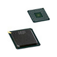
SAA7118E/V1/M5.557 NXP Semiconductors, SAA7118E/V1/M5.557 Datasheet - Page 23

SAA7118E/V1/M5.557
Manufacturer Part Number
SAA7118E/V1/M5.557
Description
Manufacturer
NXP Semiconductors
Datasheet
1.SAA7118EV1M5.557.pdf
(177 pages)
Specifications of SAA7118E/V1/M5.557
Adc/dac Resolution
9b
Screening Level
Commercial
Package Type
LBGA
Pin Count
156
Lead Free Status / RoHS Status
Compliant
- Current page: 23 of 177
- Download datasheet (972Kb)
NXP Semiconductors
SAA7118_7
Product data sheet
The increment generation circuit produces the Discrete Time Oscillator (DTO) increment
for both subcarrier generation blocks. It contains a division by the increment of the
line-locked clock generator to create a stable phase-locked sine signal under all conditions
(e.g. for non-standard signals).
The PAL delay line block eliminates crosstalk between the chrominance channels in
accordance with the PAL standard requirements. For NTSC color standards the delay line
can be used as an additional vertical filter. If desired, it can be switched off by DCVF = 1.
It is always disabled during VBI or raw data lines programmable by the LCRn registers
(subaddresses 41h to 57h); see
SECAM recombination (cross-over switches).
•
•
Loop filter chrominance PLL (only active for PAL/NTSC standards)
PAL/SECAM sequence detection, H / 2-switch generation
Rev. 07 — 7 July 2008
Multistandard video decoder with adaptive comb filter
Section
8.3. The embedded line delay is also used for
SAA7118
© NXP B.V. 2008. All rights reserved.
23 of 177
Related parts for SAA7118E/V1/M5.557
Image
Part Number
Description
Manufacturer
Datasheet
Request
R
Part Number:
Description:
Video ICs COMPONENT + VIDEO PROCESSOR
Manufacturer:
NXP Semiconductors

Part Number:
Description:
IC VIDEO DECOD W/FILTER 156LBGA
Manufacturer:
NXP Semiconductors
Datasheet:
Part Number:
Description:
IC VIDEO DECOD W/FILTER 156LBGA
Manufacturer:
NXP Semiconductors

Part Number:
Description:
IC VIDEO DECODER W/FILTER 156BGA
Manufacturer:
NXP Semiconductors

Part Number:
Description:
IC VIDEO DECODR W/FILTER 156LBGA
Manufacturer:
NXP Semiconductors

Part Number:
Description:
IC VIDEO DECODR W/FILTER 156LBGA
Manufacturer:
NXP Semiconductors
Part Number:
Description:
Video ICs VIDEO DECODER W/FILTER
Manufacturer:
NXP Semiconductors

Part Number:
Description:
Video ICs COMPONENT VID DECODER W/COMB F
Manufacturer:
NXP Semiconductors
Datasheet:

Part Number:
Description:
Manufacturer:
NXP Semiconductors
Datasheet:
Part Number:
Description:
NXP Semiconductors designed the LPC2420/2460 microcontroller around a 16-bit/32-bitARM7TDMI-S CPU core with real-time debug interfaces that include both JTAG andembedded trace
Manufacturer:
NXP Semiconductors
Datasheet:

Part Number:
Description:
NXP Semiconductors designed the LPC2458 microcontroller around a 16-bit/32-bitARM7TDMI-S CPU core with real-time debug interfaces that include both JTAG andembedded trace
Manufacturer:
NXP Semiconductors
Datasheet:
Part Number:
Description:
NXP Semiconductors designed the LPC2468 microcontroller around a 16-bit/32-bitARM7TDMI-S CPU core with real-time debug interfaces that include both JTAG andembedded trace
Manufacturer:
NXP Semiconductors
Datasheet:
Part Number:
Description:
NXP Semiconductors designed the LPC2470 microcontroller, powered by theARM7TDMI-S core, to be a highly integrated microcontroller for a wide range ofapplications that require advanced communications and high quality graphic displays
Manufacturer:
NXP Semiconductors
Datasheet:


