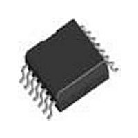
MF6CWM-100 National Semiconductor, MF6CWM-100 Datasheet

MF6CWM-100
Specifications of MF6CWM-100
Available stocks
Related parts for MF6CWM-100
MF6CWM-100 Summary of contents
Page 1
... DC gain of 1 V/V allows cascading MF6 sections for higher order Block and Connection Diagrams All Packages DS005065-2 Top View Order Number MF6CWM-50 or MF6CWM-100 See NS Package Number M14B TRI-STATE ® registered trademark of National Semiconductor Corporation. © 1999 National Semiconductor Corporation DS005065 filtering ...
Page 2
... V − 0.2V 0.2V Operating Ratings Temperature Range 500 mW MF6CWM-50, MF6CWM-100 −65˚C to +150˚C Supply Voltage (V 800V 250 kHz (Note 3) unless otherwise specified. Boldface limits apply for T CLK Conditions Typical (Note 8) Min Max Min Max ...
Page 3
Filter Electrical Characteristics The following specifications apply for f CLK = T = 25˚ all other limits T MAX A J Parameter + − = +2.5V −2.5V V Total Supply Current Maximum Filter Output Clock ...
Page 4
Op Amp Electrical Characteristics Boldface limits apply for MIN MAX Parameter + − = +2.5V −2.5V V Input Bias Current CMRR (Op-Amp # 2 Only) Output Voltage Swing Maximum Output Short Source Circuit Current (Note ...
Page 5
... Note 14: The maximum power dissipation must be derated at elevated temperatures and is dictated allowable power dissipation at any temperature 125˚C, and the typical junction-to-ambient thermal resistance is 78˚C/W. For the MF6CJ this number decreases to 62˚C/W. For MF6CWM, T JMAX Typical Performance Characteristics Schmitt Trigger Threshold Voltage ...
Page 6
Typical Performance Characteristics Positive Voltage Swing vs Power Supply Voltage (Op Amp Output) DS005065-46 Negative Voltage Swing vs Power Supply Voltage (Filter and Op Amp Outputs) DS005065-49 Power Supply Current vs Temperature DS005065-52 www.national.com (Continued) Positive Voltage Swing vs Power ...
Page 7
Typical Performance Characteristics f /f Deviation CLK c vs Temperature DS005065- Deviation CLK c vs Temperature DS005065-58 DC Gain Deviation vs Power Supply Voltage DS005065-61 (Continued Deviation CLK c vs Power Supply Voltage DS005065- ...
Page 8
Typical Performance Characteristics DC Gain Deviation vs Power Supply Voltage DS005065-64 Crosstalk Test Circuits Pin Descriptions (Pin Numbers) Pin Description FILTER OUT The output of the lowpass filter. It (3) will typically sink 0.9 mA and source 3 mA and ...
Page 9
Pin Descriptions (Pin Numbers) (Continued) Pin Description AGND (5) The analog ground pin. This pin sets the DC bias level for the filter section and the non-inverting input of Op-Amp # 1 and must be tied to the system ground ...
Page 10
MF6 Application Hints The MF6 is comprised of a non-inverting unity gain lowpass sixth order Butterworth switched capacitor filter section and two undedicated CMOS Op-Amps. The switched capacitor topology makes the cutoff frequency (where the gain drops 3.01 dB ...
Page 11
MF6 Application Hints FIGURE 2. Dual Supply Operation MF6 Driven with CMOS Logic Level Clock (V 0.8 V and V 0.2 V where (Continued) FIGURE 3. Dual Supply Operation DS005065-3 MF6 Driven with TTL ...
Page 12
MF6 Application Hints www.national.com (Continued) a) Resistor Biasing of AGND b) Using Op-Amp 2 to Buffer AGND FIGURE 4. Single Supply Operation 12 DS005065-14 DS005065-15 ...
Page 13
MF6 Application Hints Schmitt-trigger threshold voltage levels can change signifi- cantly causing the R/C oscillator’s frequency to vary greatly from part to part. Where accuracy required an external clock can be c used to drive the ...
Page 14
MF6 Application Hints (where T equals one clock period) or The equivalent input resistor (R ) then can be defined as in The input capacitor for the MF6-50 and 1 pF for the MF6-100, so for ...
Page 15
MF6 Application Hints DS005065-23 ± FIGURE 10. MF6-50 2.5V Supplies Amplitude Response 2.0 Designing with the MF6 Given any lowpass filter specification two equations will come in handy in trying to determine whether the MF6 will do the job. ...
Page 16
Designing with the MF6 2.3 IMPLEMENTING A “NOTCH” FILTER WITH THE MF6 A “notch” filter with attenuation can be obtained by using one of the Op-Amps, available in the MF6, and three external resistors. The circuit ...
Page 17
Designing with the MF6 FIGURE 16. MF6-50 “Notch” Filter Amplitude Response 2.4 CHANGING CLOCK FREQUENCY INSTANTANEOUSLY The MF6 will respond favorably to a sudden change in clock frequency. Distortion in the output signal occurs at the tran- sition of ...
Page 18
Designing with the MF6 = 1.5 kHz (scope time base = 2 ms/div FIGURE 17. MF6-50 Abrupt Clock Frequency Change 2.5 ALIASING CONSIDERATIONS Aliasing effects have to be taken into consideration when in- put signal frequencies exceed ...
Page 19
Designing with the MF6 Note: The parallel combination of R (if used), R and FIGURE 20. Second Order Butterworth Anti-Aliasing Filter Using Uncommitted Op-Amp # 2 (Continued) should order not to load ...
Page 20
... Physical Dimensions inches (millimeters) unless otherwise noted Order Number MF6CWM-50 or MF6CWM-100 LIFE SUPPORT POLICY NATIONAL’S PRODUCTS ARE NOT AUTHORIZED FOR USE AS CRITICAL COMPONENTS IN LIFE SUPPORT DEVICES OR SYSTEMS WITHOUT THE EXPRESS WRITTEN APPROVAL OF THE PRESIDENT AND GENERAL COUNSEL OF NATIONAL SEMICONDUCTOR CORPORATION. As used herein: 1 ...


