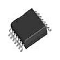
MF6CWM-100 National Semiconductor, MF6CWM-100 Datasheet - Page 9

MF6CWM-100
Manufacturer Part Number
MF6CWM-100
Description
Manufacturer
National Semiconductor
Datasheet
1.MF6CWM-100.pdf
(20 pages)
Specifications of MF6CWM-100
Architecture
Switched Capacitor
Dual Supply Voltage (typ)
±3/±5V
Power Supply Requirement
Single/Dual
Single Supply Voltage (min)
5V
Dual Supply Voltage (min)
±2.5V
Operating Temperature (min)
0C
Operating Temperature (max)
70C
Operating Temperature Classification
Commercial
Package Type
SOIC W
Filter Type
Low Pass Filter
Lead Free Status / RoHS Status
Not Compliant
Available stocks
Company
Part Number
Manufacturer
Quantity
Price
Company:
Part Number:
MF6CWM-100
Manufacturer:
NS
Quantity:
5 510
Company:
Part Number:
MF6CWM-100
Manufacturer:
QTC
Quantity:
5 510
Part Number:
MF6CWM-100
Manufacturer:
NS/国半
Quantity:
20 000
Pin Descriptions
Pin
AGND (5)
V
INV1 (13)
V
INV2 (14),
NINV2 (1)
V
CLK IN (9)
CLK R (11)
L. Sh (12)
O1
O2
+
(6), V
(4),
(2),
−
(10)
Description
The analog ground pin. This pin sets
the DC bias level for the filter section
and the non-inverting input of
Op-Amp # 1 and must be tied to the
system ground for split supply
operation or to mid-supply for single
supply operation (see section 1.2).
When tied to mid-supply this pin
should be well bypassed.
V
inverting input of Op-Amp # 1. The
non-inverting input of this Op-Amp is
internally connected to the AGND
pin.
V
inverting input, and NINV2 is the
non-inverting input of Op-Amp # 2.
The positive and negative supply
pins. The total power supply range is
5V to 14V. Decoupling these pins
with 0.1 µF capacitors is highly
recommended.
A CMOS Schmitt-trigger input to be
used with an external CMOS logic
level clock. Also used for
self-clocking Schmitt-trigger oscillator
(see section 1.1).
A TTL logic level clock input when in
split supply operation (
ground. This pin becomes a low
impedance output when L. Sh is tied
to V
the CLK IN pin for a self clocking
Schmitt-trigger oscillator (see section
1.1).
Level shift pin, selects the logic
threshold levels for the desired
clock. When tied to V
internal tri-state
between the Schmitt trigger and the
internal clock level shift stage thus
enabling the CLK IN Schmitt-trigger
input and making the CLK R pin a
low impedance output.
When the voltage level at this input
exceeds [25%(V
internal tri-state buffer is disabled
allowing the CLK R pin to become
the clock input for the internal clock
level shift stage. The CLK R
threshold level is now 2V above the
voltage applied to the L. Sh pin.
Driving the CLK R pin with TTL logic
levels can be accomplished through
the use of split supplies and by tying
the L. Sh pin to system ground.
±
O1
O2
7V) and L. Sh tied to system
−
is the output and INV1 is the
is the output, INV2 is the
. Also used in conjunction with
(Pin Numbers) (Continued)
®
+
buffer stage
− V
−
−
) + V
±
it enables an
2.5V to
−
] the
9
www.national.com


