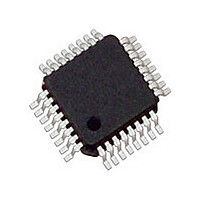
MC33911G5ACR2 Freescale, MC33911G5ACR2 Datasheet - Page 26

MC33911G5ACR2
Manufacturer Part Number
MC33911G5ACR2
Description
Manufacturer
Freescale
Datasheet
1.MC33911G5ACR2.pdf
(92 pages)
Specifications of MC33911G5ACR2
Turn Off Delay Time
10us
Number Of Drivers
2
Operating Temperature (min)
-40C
Operating Temperature (max)
125C
Operating Temperature Classification
Automotive
Lead Free Status / RoHS Status
Compliant
Available stocks
Company
Part Number
Manufacturer
Quantity
Price
Company:
Part Number:
MC33911G5ACR2
Manufacturer:
Freescale Semiconductor
Quantity:
10 000
- Current page: 26 of 92
- Download datasheet (2Mb)
VOLTAGE SENSE PIN (VSENSE)
is protected against battery reverse connection. The voltage
present in this input is scaled down by an internal voltage
divider, and can be routed to the ADOUT0 output pin and
used by the MCU to read the battery voltage.
+40 V and down to -27 V, allowing this pin to be connected
directly to the battery line. It is strongly recommended to
connect a 10 kohm resistor in series with this pin for
protection purposes.
26
33911
FUNCTIONAL DESCRIPTION
FUNCTIONAL PIN DESCRIPTION
This input can be connected directly to the battery line. It
The ESD structure on this pin allows for excursion up to
+5.0 V MAIN REGULATOR OUTPUT PIN (VDD)
stabilize the regulated output voltage. The VDD pin is
intended to supply a microcontroller. The pin is current limited
against shorts to GND and over-temperature protected.
with its full drive capabilities and the output current is limited.
down.
An external capacitor has to be placed on the VDD pin to
During Stop mode, the voltage regulator does not operate
During Sleep mode, the regulator output is completely shut
Analog Integrated Circuit Device Data
Freescale Semiconductor
Related parts for MC33911G5ACR2
Image
Part Number
Description
Manufacturer
Datasheet
Request
R
Part Number:
Description:
Mc33911 Lin System Basis Chip With Dc Motor Pre-driver
Manufacturer:
Freescale Semiconductor, Inc
Datasheet:

Part Number:
Description:
TOWER ELEVATOR BOARDS HARDWARE
Manufacturer:
Freescale Semiconductor
Datasheet:

Part Number:
Description:
TOWER SERIAL I/O HARDWARE
Manufacturer:
Freescale Semiconductor
Datasheet:

Part Number:
Description:
LCD MODULE FOR TWR SYSTEM
Manufacturer:
Freescale Semiconductor
Datasheet:

Part Number:
Description:
DAUGHTER LCD WVGA I.MX51
Manufacturer:
Freescale Semiconductor
Datasheet:

Part Number:
Description:
TOWER SYSTEM BOARD MPC5125
Manufacturer:
Freescale Semiconductor
Datasheet:

Part Number:
Description:
KIT EVALUATION I.MX51
Manufacturer:
Freescale Semiconductor
Datasheet:

Part Number:
Description:
KIT DEVELOPMENT WINCE IMX25
Manufacturer:
Freescale Semiconductor
Datasheet:

Part Number:
Description:
TOWER SYSTEM KIT MPC5125
Manufacturer:
Freescale Semiconductor
Datasheet:

Part Number:
Description:
TOWER SYSTEM BOARD K40X256
Manufacturer:
Freescale Semiconductor
Datasheet:

Part Number:
Description:
TOWER SYSTEM KIT K40X256
Manufacturer:
Freescale Semiconductor
Datasheet:

Part Number:
Description:
Microcontrollers (MCU) MX28 PLATFORM DEV KIT
Manufacturer:
Freescale Semiconductor
Datasheet:

Part Number:
Description:
MCU, MPU & DSP Development Tools IAR KickStart Kit for Kinetis K60
Manufacturer:
Freescale Semiconductor
Datasheet:

Part Number:
Description:
24BIT HDMI MX535/08
Manufacturer:
Freescale Semiconductor
Datasheet:
Part Number:
Description:
Manufacturer:
Freescale Semiconductor, Inc
Datasheet:


