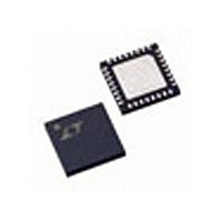
LTC3770EUH#TR Linear Technology, LTC3770EUH#TR Datasheet - Page 8

LTC3770EUH#TR
Manufacturer Part Number
LTC3770EUH#TR
Description
Manufacturer
Linear Technology
Datasheet
1.LTC3770EUHTR.pdf
(24 pages)
Specifications of LTC3770EUH#TR
Lead Free Status / RoHS Status
Not Compliant
Available stocks
Company
Part Number
Manufacturer
Quantity
Price
LTC3770
PIN FUNCTIONS
sets the ramp rate for the output voltage. When the IC is
confi gured to be the slave of two outputs, the V
of the master IC is reproduced by a resistor divider and
applied to this pin. An internal 1.4μA soft-start current is
charging this pin during the soft-start phase.
PLLFLTR (Pin 12/Pin 15): The Phase-Locked Loop’s
Lowpass Filter is Tied to This Pin. The voltage at this pin
defaults to 1.18V when the IC is not synchronized with
an external clock at the PLLIN pin.
PLLIN (Pin 13/Pin 16): External Synchronization Input to
Phase Detector. This pin is internally terminated to SGND
with a 50k resistor.
V
to PGND with a capacitor (0.1μF to 1μF).
V
Normally this pin is tied to V
applications when the IC is powered from a separate
supply, V
sense the V
the SSOP package.
ZV
Input. Under normal conditions this pin should always be
connected to INTV
Z1 (Pin 17/Pin 19): Post-Package Zener-Trim Control.
This pin is a multifunctional pin used in production for
post-package trimming and tracking. Ground this pin under
normal soft-start operation. Connecting this pin to INTV
will turn off the soft-start current during tracking.
Z2 (Pin 18/Pin 20): Post-Package Zener-Trim Control.
This pin is used in production for Post-Package trimming.
Ground this pin or tie to INTV
INTV
control circuits are powered from this voltage. Decouple this
pin to PGND with a minimum of 4.7μF low ESR tantalum
or ceramic capacitor.
DRV
Must be connected to INTV
7V at this pin. This pin is co-bonded to INTV
in the SSOP package.
8
IN
INSNS
IN
(Pin 14/Pin 17): Main Input Supply. Decouple this pin
CC
CC
(Pin 16/Pin 18): Post-Package Zener-Trim Voltage
(Pin 20) UH Package Gate: Driver Voltage Input.
(Pin 15) UH Package: V
(Pin 19/Pin 21): Internal 5V Regulator Output. The
INSNS
IN
voltage. The pin is co-bonded with V
is tied to the upper MOSFET supply to
CC
.
(UH Package/G Package)
CC
CC
externally. Do not exceed
IN
under normal operation.
IN
. However, in certain
Voltage Sense Input.
CC
FB
internally
voltage
IN
CC
in
BG (Pin 21/Pin 22): Bottom Gate Driver Output. This pin
drives the gate of the bottom N-channel MOSFET between
ground and INTV
PGND (Pin 22/Pin 23): Power Ground. Connect this pin
closely to the source of the bottom N-channel MOSFET,
the (–) terminal of CV
SENSE
Input. The (–) input to the current comparator is used
to accurately Kelvin sense the bottom side of the sense
resistor or MOSFET. This pin is co-bonded with PGND
internally in the SSOP package.
SENSE
Input. The (+) input to the current comparator is normally
connected to the SW node unless using a sense resistor.
This pin is co-bonded with SW internally in the SSOP
package.
SW (Pin 25/Pin 24): Switch Node. The (–) terminal of the
boot-strap capacitor CB connects here. This pin swings
from a diode voltage drop below ground up to V
TG (Pin 26/Pin 25): Top Gate Drive Output. This pin drives
the top N-channel MOSFET with a voltage swing equal to
INTV
BOOST (Pin 27/Pin 26): Boosted Floating Driver Supply.
The (+) terminal of the boot-strap capacitor CB connects
here. This pin swings from a diode voltage drop below
INTV
Z0 (Pin 28/Pin 27): Dead Time Control Input. Applying a
DC voltage will vary the dead time between TG-Low and
BG-High transition. Do not force a voltage higher than
5V on this pin.
FCB (Pin 29/Pin 28): Forced Continuous Input. Connect
this pin to SGND to forced continuous synchronization
operation at low load, to INTV
mode operation at low load or to a resistive divider from
a secondary output when using a secondary winding.
RUN (Pin 30/Pin 1): Run Control Input. A voltage above
1.5V turns on the IC. Forcing this pin below 1.5V shuts
down the device.
CC
CC
–
+
, superimposed on the switch node voltage SW.
up to V
(Pin 23) UH Package: Current Sense Comparator
(Pin 24) UH Package: Current Sense Comparator
IN
CC
+ INTV
.
CC
CC
and the (–) terminal of C
.
CC
to enable discontinuous
IN
IN
.
.
3770fc


