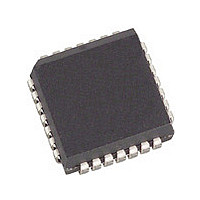
CY7C266-20JC Cypress Semiconductor Corp, CY7C266-20JC Datasheet
CY7C266-20JC
Specifications of CY7C266-20JC
Available stocks


Related parts for CY7C266-20JC

CY7C266-20JC Summary of contents
Page 1
... The memory cells utilize proven EPROM floating-gate programming algorithms. The CY7C266 is a plug-in replacement for EPROM devices. The EPROM cell requires only 12.5V for the super voltage and low-current requirements allow for gang programming. The EPROM cells allow for each memory location to be tested 100%, as each location is written into, erased, and repeatedly exercised prior to encapsulation ...
Page 2
... CC V < V < OUT OH Output Disabled V = Max GND CC OUT V = Max 2.0V, Com’ OUT Chip Enable Inactive, Com’l CE > OUT CY7C266 7C266-45 Unit 45 ns 100 Ambient Temperature V CC ° ° + ± 10% 7C266-20 7C266-25 Unit Min. Max. Min. Max. 2.4 2.4 V 2.4 ...
Page 3
... Output Disabled V = Max GND CC OUT V = Max 2.0V, Com’ OUT Chip Enable Inactive, Com’l CE > OUT Test Conditions T = 25° MHz 5.0V CC CY7C266 7C266-45 Unit Min. Max. 2.4 V 0.4 V 2.0 V 0.8 V –10 +10 mA Note 3 –10 +10 mA –20 –90 mA 100 Max. Unit ...
Page 4
... R1 500Ω (658Ω MIL) 5V 3.0V GND R2 333Ω (403Ω MIL) INCLUDING JIG AND SCOPE (b) High Z Load R1 250Ω 5V R2167 Ω INCLUDING JIG AND SCOPE (d) High Z Load [2] 7C266-20 Min. Max CY7C266 90% 90% 10% 10% < 7C266-25 7C266-45 Min. Max. Min. Max Page < Unit ns ...
Page 5
... Wsec/cm 2 ultraviolet lamp with a 12 mW/cm power rating, the exposure time would be approximately 35 minutes. The CY7C266 needs to be within 1 inch of the lamp during erasure. Permanent damage may Table 1. Mode Selection Mode Normal Operation ...
Page 6
... CYCLE PERIOD 1.05 1.00 0.95 0. 25°C 0.80 A 0.75 0.70 2.0 3.0 4 CYCLE PERIOD (ns) CY7C266 NORMALIZED ACCESS TIME vs. SUPPLY VOLTAGE 1.2 1.0 0.8 0 25°C A 0.4 4.0 4.5 5.0 5.5 6.0 SUPPLY VOLTAGE(V) TYPICAL ACCESS TIME CHANGE vs. OUTPUT LOADING 35 30 ...
Page 7
... Ordering Code 20 CY7C266 20JC - CY7C266 20WC - Package Diagrams Figure 2. 28-Lead(600-Mil) CerDIP D16 Document #: 38-04005 Rev. *C Package Package Type Name J64 28-Lead Plastic Leaded Chip Carrier W16 28-Lead (600-Mil) Windowed CerDIP MIL-STD-1835 D-10 Config. A CY7C266 Operating Range Commercial 51-80019-** Page [+] Feedback ...
Page 8
... Package Diagrams (continued) Figure 3. 32-Pin Rectangular Leadless Chip Carrier L55 Document #: 38-04005 Rev. *C MIL-STD-1835 C-12 51-80068-** CY7C266 Page [+] Feedback ...
Page 9
... Document #: 38-04005 Rev 0.530 0.550 28 0.070 0.090 SEATING PLANE 1.380 1.480 0.140 0.195 0.015 0.060 0.055 0.014 0.065 0.022 CY7C266 MIN. DIMENSIONS IN INCHES MAX. REFERENCE JEDEC Ms-020 0.600 0.625 0.009 3° MIN. 0.012 0.610 0.700 51-85017-*B Page [+] Feedback ...
Page 10
... Package Diagrams (continued) Figure 5. 32-Pin Windowed Rectangular Leadless Chip Carrier Q55 Document #: 38-04005 Rev. *C MIL-STD-1835 C-12 51-80103-*A CY7C266 Page [+] Feedback ...
Page 11
... The inclusion of Cypress products in life-support systems application implies that the manufacturer assumes all risk of such use and in doing so indemnifies Cypress against all charges. MIL-STD-1835 D-10 Config. A CY7C266 51-80020-** Page ...
Page 12
... Document History Page Document Title: CY7C266 Power Switched and Reprogrammable PROM Document Number: 38-04005 Issue REV. ECN NO. Date ** 113861 03/08/02 *A 118897 10/09/02 *B 122246 12/27/02 *C 499538 See ECN Document #: 38-04005 Rev. *C Orig. of Description of Change Change DSG Changed from Spec number: 38-00086 to 38-04005 ...