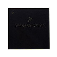
DSP56301VF100 Freescale, DSP56301VF100 Datasheet - Page 15

DSP56301VF100
Manufacturer Part Number
DSP56301VF100
Description
Manufacturer
Freescale
Datasheet
1.DSP56301VF100.pdf
(124 pages)
Specifications of DSP56301VF100
Device Core Size
24b
Format
Fixed Point
Clock Freq (max)
100MHz
Mips
100
Device Input Clock Speed
100MHz
Ram Size
24KB
Operating Supply Voltage (typ)
3.3V
Operating Supply Voltage (min)
3V
Operating Supply Voltage (max)
3.6V
Operating Temp Range
-40C to 100C
Operating Temperature Classification
Industrial
Mounting
Surface Mount
Pin Count
252
Package Type
MA-BGA
Lead Free Status / RoHS Status
Not Compliant
Available stocks
Company
Part Number
Manufacturer
Quantity
Price
Company:
Part Number:
DSP56301VF100
Manufacturer:
Freescale Semiconductor
Quantity:
10 000
Part Number:
DSP56301VF100
Manufacturer:
MOTOROLA/摩托罗拉
Quantity:
20 000
1.7.2
HI32 signal functions vary according to the programmed configuration of the interface as determined by the 24-bit
DSP Control Register (DCTR). Refer to the
Freescale Semiconductor
Asynchronous write to host
vector
HAD[0–7]
HA[3–10]
PB[0–7]
HAD[8–15]
HD[0–7]
PB[8–15]
HC[0–3]/
HBE[0–3]
HA[0–2]
PB[16–19]
Signal Name
Action
Host Port Configuration
Input/Output
Input
Input or Output
Input/Output
Input/Output
Input or Output
Input/Output
Input
Input or Output
Type
Table 1-10.
Change the Host Vector (HV) register only when the Host Command bit (HC) is clear. This practice
guarantees that the DSP interrupt control logic receives a stable vector.
Tri-stated
Tri-stated
Tri-stated
State During
Reset
DSP56301 Technical Data, Rev. 10
Host Port Usage Considerations (Continued)
Table 1-11.
DSP56301
Host Address/Data 0–7
When the HI32 is programmed to interface with a PCI bus and the HI function
is selected, these signals are lines 0–7 of the Address/Data bus.
Host Address 3–10
When HI32 is programmed to interface with a universal, non-PCI bus and the
HI function is selected, these signals are lines 3–10 of the Address bus.
Port B 0–7
When the HI32 is configured as GPIO through the DCTR, these signals are
individually programmed through the HI32 Data Direction Register (DIRH).
These inputs are 5 V tolerant.
Host Address/Data 8–15
When the HI32 is programmed to interface with a PCI bus and the HI function
is selected, these signals are lines 8–15 of the Address/Data bus.
Host Data 0–7
When HI32 is programmed to interface with a universal non-PCI bus and the
HI function is selected, these signals are lines 0–7 of the Data bus.
Port B 8–15
When the HI32 is configured as GPIO through the DCTR, these signals are
individually programmed through the HI32 DIRH.
These inputs are 5 V tolerant.
Command 0–3/Byte Enable 0–3
When the HI32 is programmed to interface with a PCI bus and the HI function
is selected, these signals are lines 0–7 of the Address/Data bus.
Host Address 0–2
When HI32 is programmed to interface with a universal, non-PCI bus and the
HI function is selected, these signals are lines 0–2 of the Address bus.
The fourth signal in this set should connect to a pull-up resistor or directly to
V
Port B 16–19
When the HI32 is configured as GPIO through the DCTR, these signals are
individually programmed through the HI32 DIRH.
These inputs are 5 V tolerant.
CC
when a non-PCI bus is used.
User’s Manual for details on HI32 configuration registers.
Host Interface
Description
Signal Description
Host Interface (HI32)
1-11


