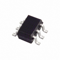
ADCMP608BKSZ-R2 Analog Devices Inc, ADCMP608BKSZ-R2 Datasheet - Page 8

ADCMP608BKSZ-R2
Manufacturer Part Number
ADCMP608BKSZ-R2
Description
Comparator Single R-R I/P 5.5V 6-Pin SC-70 T/R
Manufacturer
Analog Devices Inc
Type
General Purposer
Datasheet
1.ADCMP608BKSZ-REEL7.pdf
(12 pages)
Specifications of ADCMP608BKSZ-R2
Package
6SC-70
Rail To Rail
Rail to Rail Input
Number Of Channels Per Chip
1
Minimum Single Supply Voltage
2.5 V
Power Supply Type
Single
Number Of Elements
1
Output Type
CMOS, Rail-to-Rail, TTL
Voltage - Supply
2.5 V ~ 5.5 V
Mounting Type
Surface Mount
Package / Case
6-TSSOP, SC-88, SOT-363
Comparator Type
High Speed
No. Of Comparators
1
Response Time
40ns
Ic Output Type
CMOS, MOS, Open-Collector / Drain, TTL
Supply Current
550µA
Supply Voltage Range
2.5V To 5.5V
Rohs Compliant
Yes
Output Compatibility
CMOS, TTL
Number Of Elements
1
Technology
CMOS
Input Offset Voltage
3mV
Single Supply Voltage (typ)
3/5V
Dual Supply Voltage (typ)
Not RequiredV
Supply Current (max)
1.3mA
Power Supply Requirement
Single
Common Mode Rejection Ratio
45dB
Voltage Gain In Db
80dB
Power Supply Rejection Ratio
50dB
Single Supply Voltage (min)
2.5V
Single Supply Voltage (max)
5.5V
Dual Supply Voltage (min)
Not RequiredV
Dual Supply Voltage (max)
Not RequiredV
Power Dissipation
2mW
Operating Temp Range
-40C to 125C
Operating Temperature Classification
Automotive
Mounting
Surface Mount
Pin Count
6
Package Type
SC-70
Lead Free Status / RoHS Status
Lead free / RoHS Compliant
Lead Free Status / RoHS Status
Lead free / RoHS Compliant
Available stocks
Company
Part Number
Manufacturer
Quantity
Price
Part Number:
ADCMP608BKSZ-R2
Manufacturer:
ADI/亚德诺
Quantity:
20 000
ADCMP608
INPUT VOLTAGE
Q OUTPUT
INPUT VOLTAGE
Q OUTPUT
Figure 10. Propagation Delay—Overdrive Dispersion
Figure 11. Propagation Delay—Slew Rate Dispersion
10V/ns
1V/ns
500mV OVERDRIVE
10mV OVERDRIVE
DISPERSION
DISPERSION
V
V
N
N
± V
± V
OS
OS
Rev. 0 | Page 8 of 12
CROSSOVER BIAS POINT
Rail-to-rail inputs of this type, in both op amps and comparators,
have a dual front-end design. Certain devices are active near the
V
mined point in the common-mode range, a crossover occurs. At
this point, normally V
and there are changes in measured offset voltages and currents.
The ADCMP608 slightly elaborates on this scheme. Crossover
points can be found at approximately 0.8 V and 1.6 V.
MINIMUM INPUT SLEW RATE REQUIREMENT
With the rated load capacitance and normal good PC board
design practice, as discussed in the
section, these comparators should be stable at any input slew
rate with no hysteresis. Broadband noise from the input stage is
observed in place of the violent chattering seen with most other
high speed comparators. With additional capacitive loading or
poor bypassing, oscillation may be encountered. These oscilla-
tions are due to the high gain bandwidth of the comparator in
combination with feedback through parasitics in the package
and PC board. In many applications, chattering is not harmful.
CC
rail and others are active near the V
CC
/2, the direction of the bias current reverses
Optimizing Performance
EE
rail. At some predeter-


