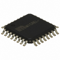
SY100EP195VTG TR Micrel Inc, SY100EP195VTG TR Datasheet - Page 13

SY100EP195VTG TR
Manufacturer Part Number
SY100EP195VTG TR
Description
IC DELAY LINE 3.3/5V 32-TQFP
Manufacturer
Micrel Inc
Series
100EPr
Type
Programmable Delay Chipr
Datasheet
1.SY100EP195VTG.pdf
(18 pages)
Specifications of SY100EP195VTG TR
Input
CMOS, ECL, TTL
Output
ECL
Frequency - Max
2.5GHz
Voltage - Supply
3 V ~ 3.6 V, 4.5 V ~ 5.5 V
Operating Temperature
-40°C ~ 85°C
Mounting Type
Surface Mount
Package / Case
32-TQFP, 32-VQFP
Frequency-max
2.5GHz
Lead Free Status / RoHS Status
Lead free / RoHS Compliant
Other names
SY100EP195VTGTR
SY100EP195VTGTR
SY100EP195VTGTR
M9999-120505
hbwhelp@micrel.com or (408) 955-1690
Micrel, Inc.
delay of a PECL or NECL input signal by any amount between
about 2.2ns and 12.2ns. A 10-bit digital control register affords
delay steps of approximately 10ps.
chain and a set of fixed delay elements. Under digital control,
various subsets of the delay elements are included in the
signal chain. To simplify interfacing, the 10-bit digital delay
control word interfaces to PECL, CMOS, or TTL interface
standards.
SY100EP195V has a minimum delay of about 2.2ns. Delays
below this value are not possible. In addition, when cascading
multiple SY100EP195V to extend the delay range, the
minimum delay is about 2.2ns times the number of
SY100EP195V in cascade. An eleventh control bit, D[10],
along with the CASCADE and /CASCADE outputs and the
SETMIN and SETMAX inputs, simplifies the task of cascading.
Signal Path Logic Standard
LVPECL, or NECL signals, as shown in Table 6. The choice
of signal path logic standard may limit possible choices for
the delay control inputs, D.
Input Enable
the input is effectively gated out, just as if a logic low was
being provided to SY100EP195V.
Digital Control Latch
into its internal 11-bit latch, 10 bits for D[0:9], and an extra bit
for the D[10] cascade control. The LEN input controls the
action of this latch, as per Table 2.
NECL, the same as the IN, /IN signal pair. The 11-bit delay
control word, however, may also be CMOS or TTL.
D[0:9], where D[0] is the least significant bit, and D[9] is the
most significant bit. This delay from IN, /IN to Q, /Q is about:
FUNCTIONAL DESCRIPTION
SY100EP195V is a programmable delay line, varying the
SY100EP195V implements the delay using a multiplexer
Since multiplexers must appear in the delay path,
The signal path, from IN, /IN to Q, /Q, interfaces to PECL,
The /EN input gates the signal at IN, /IN. When disabled,
SY100EP195V can capture the digital delay control word
Note that the LEN input is always PECL, LVPECL, or
The nominal delay value is based on the binary value in
∆t
=
2200 10 value D 9:0 , ps
+
LEN
/EN
H
H
L
L
Table 2. LEN Truth Table
Table 1. /EN Truth Table
×
(
[
]
)
Pass Through D[0:10]
Logic Low Delayed
IN, /IN Delayed
Value at Q, /Q
Latch Action
Latch D[0:10]
13
Digital Control Logic Standard
SY100EP195V may interface either to PECL, CMOS, or TTL
on its D[0:10] inputs. To this end, the V
at which the D inputs switch between logic low and logic high.
threshold to PECL (if V
Leaving V
detecting CMOS output logic levels. Leaving V
connecting V
TTL signals.
through an appropriate resistor will bias V
The value of this resistor depends on the V
indicated in Table 4.
Cascade Logic
devices in order to achieve a greater delay range. The SETMIN
and SETMAX pins accomplish this, as set out in the
applications section below. SETMIN and SETMAX override
the delay by changing the value in the D latch register. Table
5 lists the action of these pins.
When used in systems where V
As shown in Table 3, connecting V
If a 1.5V source is not available, connecting V
SY100EP195V is designed to ease cascading multiple
SETMIN
Table 3. Digital Control Standard Truth Table
H
H
L
L
Logic Standard
Table 4. Resistor Values for TTL Input
Table 5. SETMIN and SETMAX Action
ECL, PECL
CF
CMOS
CF
3.3V
5.0V
TTL
V
and V
CC
to a 1.5V source allows the D inputs to accept
EF
SETMAX
CC
open yields a threshold suitable for
H
H
L
L
is 5V) or LVPECL (if V
EE
Nominal Delay (ps)
CF
2200 + 10 × 1024
V
Resistor Value
As per D Latch
CF
connects to ground,
pin sets the threshold
1.5V Source
CF
No Connect
Not Allowed
Connection
CF
1.5kΩ
500Ω
2200
VEF
to V
at about 1.5V.
CC
SY100EP195V
EF
EF
CC
supply, as
CF
ECL Pro®
open and
sets the
is 3.3V).
to V
EE


