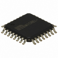
SY100EP195VTG TR Micrel Inc, SY100EP195VTG TR Datasheet - Page 15

SY100EP195VTG TR
Manufacturer Part Number
SY100EP195VTG TR
Description
IC DELAY LINE 3.3/5V 32-TQFP
Manufacturer
Micrel Inc
Series
100EPr
Type
Programmable Delay Chipr
Datasheet
1.SY100EP195VTG.pdf
(18 pages)
Specifications of SY100EP195VTG TR
Input
CMOS, ECL, TTL
Output
ECL
Frequency - Max
2.5GHz
Voltage - Supply
3 V ~ 3.6 V, 4.5 V ~ 5.5 V
Operating Temperature
-40°C ~ 85°C
Mounting Type
Surface Mount
Package / Case
32-TQFP, 32-VQFP
Frequency-max
2.5GHz
Lead Free Status / RoHS Status
Lead free / RoHS Compliant
Other names
SY100EP195VTGTR
SY100EP195VTGTR
SY100EP195VTGTR
M9999-120505
hbwhelp@micrel.com or (408) 955-1690
Micrel, Inc.
techniques, filter V
short. Use multiple vias where possible. Also, use controlled
impedance transmission lines to interface with the
SY100EP195V data inputs and outputs.
V
available for use only by the SY100EP195V. When unused,
this pin should be left unconnected. The two common uses
for V
bias inputs for AC-coupling applications.
to bias the unused input. Please refer to Figures 7. The
PECL signal driving SY100EP195V may optionally be
inverted in this case.
in Figure 8, to re-bias IN, /IN. This ensures that
SY100EP195V inputs are within its acceptable common
mode range.
limited to 0.5mA or less.
BB
APPLICATIONS INFORMATION
For best performance, use good high frequency layout
The VBB pin is an internally generated supply, and is
If IN, /IN is driven by a single-ended output, V
When the signal is AC-coupled, V
In all cases, V
Supply
BB
are to handle a single-ended PECL input, and to re-
BB
CC
supplies, and keep ground connections
current sinking our sourcing must be
IN
/IN
SY100EP195V
Figure 10b. Cascading Three SY100EP195V
BB
#3
SETMAX
Figure 10a. Cascading Two SY100EP195V
SETMIN
is used, as shown
/Q
Q
IN
/IN
SY100EP195V
#2
SETMAX
BB
SETMIN
C[11]
is used
Control Word (11bits)
Control Word (12bits)
/Q
Q
D[10]
IN
/IN
/CASCADE
CASCADE
SY100EP195V
15
#2
SETMAX
SETMIN
C[9:0]
C[10]
Setting D Input Logic Thresholds
SY100EP195V V
may accommodate CMOS and TTL level signals, as well as
PECL or LVPECL. Figures 9 show how to connect V
V
Cascading
to extend the range of delays permitted. Each additional
SY100EP195V adds about 2200ps to the minimum delay,
and adds another 10240ps to the delay range.
SY100EP195V. Using this internal circuitry, SY100EP195V
may be cascaded without any external gating.
in Figures 10. Table 7 lists the nominal delay for all the
cases that appear in Figures 10.
EF
As explained earlier, in all designs where the
Two or more SY100EP195V may be cascaded, in order
Internal cascade circuitry has been included in the
Examples of cascading 2, 3, or 4 SY100EP195V appear
/Q
Q
D[10]
D[9:0]
IN
/IN
/CASCADE
CASCADE
for all possible cases.
SY100EP195V
#1
C[9:0]
C[10]
/Q
Q
D[10]
D[9:0]
IN
/IN
/CASCADE
CASCADE
SY100EP195V
EE
#1
supply is at zero volts, the D inputs
/Q
Q
SY100EP195V
ECL Pro®
CF
and


