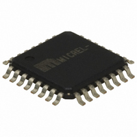
SY100EP195VTG TR Micrel Inc, SY100EP195VTG TR Datasheet - Page 3

SY100EP195VTG TR
Manufacturer Part Number
SY100EP195VTG TR
Description
IC DELAY LINE 3.3/5V 32-TQFP
Manufacturer
Micrel Inc
Series
100EPr
Type
Programmable Delay Chipr
Datasheet
1.SY100EP195VTG.pdf
(18 pages)
Specifications of SY100EP195VTG TR
Input
CMOS, ECL, TTL
Output
ECL
Frequency - Max
2.5GHz
Voltage - Supply
3 V ~ 3.6 V, 4.5 V ~ 5.5 V
Operating Temperature
-40°C ~ 85°C
Mounting Type
Surface Mount
Package / Case
32-TQFP, 32-VQFP
Frequency-max
2.5GHz
Lead Free Status / RoHS Status
Lead free / RoHS Compliant
Other names
SY100EP195VTGTR
SY100EP195VTGTR
SY100EP195VTGTR
M9999-120505
hbwhelp@micrel.com or (408) 955-1690
Micrel, Inc.
23, 25, 26, 27, 29,
PIN DESCRIPTION
30, 31, 32, 1, 2
13, 18, 19, 22
Pin Number
9, 24, 28
15, 14
20, 21
4, 5
10
11
12
16
17
3
6
7
8
CASCADE,
/CASCADE
Pin Name
SETMAX
SETMIN
IN, /IN
D[0:9]
D[10]
Q, /Q
VCC
VBB
VEF
VCF
VEE
LEN
/EN
NC
Pin Function
CMOS, ECL, or TTL Select Inputs: These digital control signals adjust the amount of
delay from IN to Q. Please refer to the “Ac Electrical Table” (page 7) and Table 7 (page
17) for delay values. Figure 9 shows how to interface these inputs to various logic family
standards. These inputs default to logic low when left unconnected. Bit 0 is the least
significant bit, and bit 9 is the most significant bit.
CMOS, ECL, or TTL Select Input: This input latches just like D[0:9] does. It drives the
CASCADE, /CASCADE differential pair. Use only when cascading two or more
SY100EP195V to extend the range of delays required.
ECL Input: This is the signal to be delayed. If this input pair is left unconnected, this is
equivalent to a logic low input.
Voltage Output: When using a single-ended logic source for IN and /IN, connect the
unused input of the differential pair to this pin. This pin can also re-bias AC-coupled inputs
to IN and /IN. When used, de-couple this pin to V
current sinking or sourcing to 0.5mA or less.
Voltage Output: Connect this pin to VCF when the D inputs are ECL. Refer to the “Digital
Control Logic Standard” section of the “Functional Description” to interface the D inputs to
CMOS or TTL.
Voltage Input: The voltage at this pin sets the logic transition threshold for the D inputs.
Most Negative Supply: Supply ground for PECL systems.
ECL Control Input: When logic low, the D inputs flow through. Any changes to the D inputs
reflect in the delay between IN, /IN and Q, /Q. When logic high, the logic values at D are
latched, and these latched bits determine the delay.
ECL Control Input: When logic high, the contents of the D register are reset. This sets the
delay to the minimum possible, equivalent to D[0:9] being set to 0000000000. When logic
low, the value of the D register, or the logic value of SETMAX determines the delay from
IN, /IN to Q, /Q. This input defaults to logic low when left unconnected.
ECL Control Input: When logic high and SETMIN is logic low, the contents of the D
register are set high, and the delay is set to one step greater than the maximum possible
with D[0:9] set to 1111111111. When logic low, the value of the D register, or the logic
value of SETMIN determines the delay from IN, /IN to Q, /Q. This input defaults to logic
low when left unconnected.
Most Positive Supply: Supply ground for NECL systems. Bypass to V
0.01µF low ESR capacitors.
100 ECL Outputs: These outputs are used when cascading two or more SY100EP195V to
extend the delay range required.
ECL Control Input: When set active low, Q, /Q are a delayed version of IN, /IN. When set
inactive high, IN, /IN are gated such that Q, /Q become a differential logic low. This input
defaults to logic low when left unconnected.
100k ECL Outputs: This signal pair is the delayed version of IN, /IN.
No Connect: Leave this pin unconnected.
3
CC
through an 0.01µF capacitor. Limit
EE
with 0.1µF and
SY100EP195V
ECL Pro®


