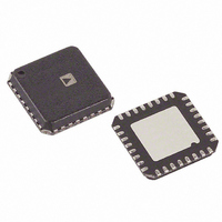
AD9513BCPZ Analog Devices Inc, AD9513BCPZ Datasheet - Page 20

AD9513BCPZ
Manufacturer Part Number
AD9513BCPZ
Description
IC CLOCK DIST 3OUT PLL 32LFCSP
Manufacturer
Analog Devices Inc
Type
Fanout Buffer (Distribution), Dividerr
Datasheet
1.AD9513BCPZ.pdf
(28 pages)
Specifications of AD9513BCPZ
Number Of Circuits
1
Ratio - Input:output
1:3
Differential - Input:output
Yes/Yes
Input
Differential
Output
CMOS, LVDS
Frequency - Max
800MHz
Voltage - Supply
3.135 V ~ 3.465 V
Operating Temperature
-40°C ~ 85°C
Mounting Type
Surface Mount
Package / Case
32-LFCSP
Frequency-max
800MHz
No. Of Multipliers / Dividers
3
No. Of Amplifiers
4
Supply Voltage Range
3.135V To 3.465V
Slew Rate
1V/ns
Operating Temperature Range
-40°C To +85°C
Digital Ic Case Style
LFCSP
Package
32LFCSP EP
Lead Free Status / RoHS Status
Lead free / RoHS Compliant
For Use With
AD9513/PCBZ - BOARD EVAL CLOCK 3CH AD9513
Lead Free Status / RoHS Status
Lead free / RoHS Compliant, Lead free / RoHS Compliant
Available stocks
Company
Part Number
Manufacturer
Quantity
Price
Company:
Part Number:
AD9513BCPZ
Manufacturer:
ADI
Quantity:
3 000
Company:
Part Number:
AD9513BCPZ
Manufacturer:
ADI
Quantity:
140
Company:
Part Number:
AD9513BCPZ-REEL7
Manufacturer:
AD
Quantity:
1 000
Company:
Part Number:
AD9513BCPZ-REEL7
Manufacturer:
ADI
Quantity:
3 000
Part Number:
AD9513BCPZ-REEL7
Manufacturer:
ADI/亚德诺
Quantity:
20 000
AD9513
Table 16. OUT0 Divide or OUT2 Divide
S9
0
1/3
2/3
1
0
1/3
2/3
1
0
1/3
2/3
1
0
1/3
2/3
1
1
DIVIDER PHASE OFFSET
The phase offset of OUT1 and OUT2 can be selected (see Table 13
to Table 15). This allows the relative phase of the outputs to be set.
After a SYNC operation (see the Synchronization section), the
phase offset word of each divider determines the number of
input clock (CLK) cycles to wait before initiating a clock output
edge. By giving each divider a different phase offset, output-to-
output delays can be set in increments of the fast clock period, t
Figure 24 shows four cases, each with the divider set to divide = 4.
By incrementing the phase offset from 0 to 3, the output is
offset from the initial edge by a multiple of t
DIVIDER OUTPUT
Duty cycle is the clock signal high time divided by the total period.
Figure 24. Phase Offset—Divider Set for Divide = 4, Phase Set from 0 to 2
CLOCK INPUT
PHASE = 0
PHASE = 1
PHASE = 2
PHASE = 3
DIV = 4
CLK
S10
0
0
0
0
1/3
1/3
1/3
1/3
2/3
2/3
2/3
2/3
1
1
1
1
0
3 × t
1
OUT0
Divide (Duty Cycle
S2 ≠ 2/3
1
2 (50%)
3 (33%)
4 (50%)
5 (40%)
6 (50%)
8 (50%)
9 (44%)
10 (50%)
12 (50%)
15 (47%)
16 (50%)
18 (50%)
24 (50%)
30 (50%)
32 (50%)
CLK
t
CLK
2
3
t
2 × t
4
CLK
CLK
5
6
7
1
8
)
9
CLK
OUT2
Divide (Duty Cycle
S2 = 2/3
7 (43%)
11 (45%)
13 (46%)
14 (50%)
17 (47%)
19 (47%)
20 (50%)
21 (48%)
22 (50%)
23 (48%)
25 (48%)
26 (50%)
27 (48%)
28 (50%)
29 (48%)
31 (48%)
10
.
11
12
13
14
1
CLK
5
Rev. 0 | Page 20 of 28
.
1
)
For example:
For Divide = 4:
The outputs can also be described as:
Setting the phase offset to Phase = 4 results in the same relative
phase as Phase = 0° or 360°.
The resolution of the phase offset is set by the fast clock period
(t
divide ratio, up to a phase offset of 15.
Phase offsets can be related to degrees by calculating the phase
step for a particular divide ratio:
Using some of the same examples:
CLK
CLK = 491.52 MHz
t
Phase Offset 0 = 0 ns
Phase Offset 1 = 2.0345 ns
Phase Offset 2 = 4.069 ns
Phase Offset 3 = 6.104 ns
Phase Offset 0 = 0°
Phase Offset 1 = 90°
Phase Offset 2 = 180°
Phase Offset 3 = 270°
Phase Step = 360°/Divide Ratio
Divide = 4
Phase Step = 360°/4 = 90°
Unique Phase Offsets in Degrees Are Phase = 0°, 90°,
Divide = 9
Phase Step = 360°/9 = 40°
Unique Phase Offsets in Degrees Are Phase = 0°, 40°, 80°,
CLK
) at CLK. The maximum unique phase offset is less than the
180°, 270°
120°, 160°, 200°, 240°, 280°, 320°
= 1/491.52 = 2.0345 ns


