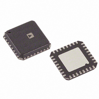
AD9513BCPZ Analog Devices Inc, AD9513BCPZ Datasheet - Page 21

AD9513BCPZ
Manufacturer Part Number
AD9513BCPZ
Description
IC CLOCK DIST 3OUT PLL 32LFCSP
Manufacturer
Analog Devices Inc
Type
Fanout Buffer (Distribution), Dividerr
Datasheet
1.AD9513BCPZ.pdf
(28 pages)
Specifications of AD9513BCPZ
Number Of Circuits
1
Ratio - Input:output
1:3
Differential - Input:output
Yes/Yes
Input
Differential
Output
CMOS, LVDS
Frequency - Max
800MHz
Voltage - Supply
3.135 V ~ 3.465 V
Operating Temperature
-40°C ~ 85°C
Mounting Type
Surface Mount
Package / Case
32-LFCSP
Frequency-max
800MHz
No. Of Multipliers / Dividers
3
No. Of Amplifiers
4
Supply Voltage Range
3.135V To 3.465V
Slew Rate
1V/ns
Operating Temperature Range
-40°C To +85°C
Digital Ic Case Style
LFCSP
Package
32LFCSP EP
Lead Free Status / RoHS Status
Lead free / RoHS Compliant
For Use With
AD9513/PCBZ - BOARD EVAL CLOCK 3CH AD9513
Lead Free Status / RoHS Status
Lead free / RoHS Compliant, Lead free / RoHS Compliant
Available stocks
Company
Part Number
Manufacturer
Quantity
Price
Company:
Part Number:
AD9513BCPZ
Manufacturer:
ADI
Quantity:
3 000
Company:
Part Number:
AD9513BCPZ
Manufacturer:
ADI
Quantity:
140
Company:
Part Number:
AD9513BCPZ-REEL7
Manufacturer:
AD
Quantity:
1 000
Company:
Part Number:
AD9513BCPZ-REEL7
Manufacturer:
ADI
Quantity:
3 000
Part Number:
AD9513BCPZ-REEL7
Manufacturer:
ADI/亚德诺
Quantity:
20 000
DELAY BLOCK
OUT2 includes an analog delay element that gives variable time
delays (ΔT) in the clock signal passing through that output.
CLOCK INPUT
The amount of delay that can be used is determined by the
output frequency. The amount of delay is limited to less than
one-half cycle of the clock period. For example, for a 10 MHz
clock, the delay can extend to the full 11.6 ns maximum. However,
for a 100 MHz clock, the maximum delay is less than 5 ns (or
half of the period).
The AD9513 allows for the selection of three full-scale delays,
1.8 ns, 6.0 ns, and 11.6 ns, set by delay full-scale (see Table 11).
Each of these full-scale delays can be scaled by 16 fine
adjustment values, which are set by the delay word (see Table 13).
The delay block adds some jitter to the output. This means that
the delay function should be used primarily for clocking digital
chips, such as FPGA, ASIC, DUC, and DDC, rather than for
supplying a sample clock for data converters. The jitter is higher
for longer full scales because the delay block uses a ramp and
trip points to create the variable delay. A longer ramp means
more noise has a chance of being introduced.
When the delay block is OFF (bypassed), it is also powered
down.
ØSELECT
÷N
Figure 25. Analog Delay Block
FULL SCALE : 1.5ns, 5ns, 10ns
FINE DELAY ADJUST
(16 STEPS)
∆T
OUT1 ONLY
CMOS
LVDS
OUTPUT
DRIVER
Rev. 0 | Page 21 of 28
OUTPUTS
Each of the three AD9513 outputs can be selected either as
LVDS differential outputs or as pairs of CMOS single-ended
outputs. If selected as CMOS, the OUT is a noninverted, single-
ended output, and OUTB is an inverted, single-ended output.
Figure 26. LVDS Output Simplified Equivalent Circuit
Figure 27. CMOS Equivalent Output Circuit
3.5mA
3.5mA
V
S
OUT1/
OUT1B
OUT
OUTB
AD9513


