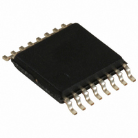
CY2DP814ZXC Cypress Semiconductor Corp, CY2DP814ZXC Datasheet - Page 4

CY2DP814ZXC
Manufacturer Part Number
CY2DP814ZXC
Description
IC CLK FANOUT BUFFER 1:4 16TSSOP
Manufacturer
Cypress Semiconductor Corp
Type
Fanout Buffer (Distribution)r
Datasheet
1.CY2DP814ZXI.pdf
(10 pages)
Specifications of CY2DP814ZXC
Package / Case
16-TSSOP
Number Of Circuits
1
Ratio - Input:output
1:4
Differential - Input:output
Yes/Yes
Input
LVDS, LVPECL, LVTTL
Output
LVPECL
Frequency - Max
450MHz
Voltage - Supply
3.135 V ~ 3.465 V
Operating Temperature
0°C ~ 70°C
Mounting Type
Surface Mount
Frequency-max
450MHz
Number Of Outputs
8
Max Input Freq
450 MHz
Supply Voltage (max)
3.465 V
Supply Voltage (min)
3.135 V
Maximum Power Dissipation
750 mW
Maximum Operating Temperature
+ 70 C
Minimum Operating Temperature
0 C
Mounting Style
SMD/SMT
Lead Free Status / RoHS Status
Lead free / RoHS Compliant
Lead Free Status / RoHS Status
Lead free / RoHS Compliant, Lead free / RoHS Compliant
Available stocks
Company
Part Number
Manufacturer
Quantity
Price
Company:
Part Number:
CY2DP814ZXC
Manufacturer:
SONY
Quantity:
7 825
Part Number:
CY2DP814ZXC
Manufacturer:
CYPRESS/赛普拉斯
Quantity:
20 000
Table 6. DC Electrical Characteristics: 3.3V–LVPECL Input
Table 7. DC Electrical Characteristics: 3.3V–LVTTL/LVCMOS Input
Table 8. DC Electrical Characteristics: 3.3V–LVPECL Output
Table 9. AC Switching Characteristics @ 3.3V V
Document Number: 38-07060 Rev. *G
I
VCM
I
I
I
V
V
I
I
I
V
V
I V
I V
Rise Time
Fall Time
V
V
I
IN [+,–] to Q[A,B] Data & Clock Speed
t
t
t
EN [1,2] to Q[A,B] Control Speed
t
Tpd
t
t
t
Parameter
IH
IL
I
IH
IL
I
Parameter
OS
PLH
PHL
PD
PE
SK(0)
SK(p)
SK(t)
Parameter
Parameter
V
IH
IL
IK
H
OH
OL
ID
OD
OC
I
I
I
Propagation Delay—Low to High
Propagation Delay—High to Low
Propagation Delay
Enable (EN) to functional operation
Functional operation to Disable
Output Skew: Skew between outputs of the same package (in phase)
Pulse Skew: Skew between opposite transitions of the same output
(t
Package Skew: Skew between outputs of different packages at the
same power supply voltage, temperature and package type. Same
input signal level and output load.
Driver Differential Output Voltage p-p
Driver common-mode p-p
Differential 20% to 80%
Output High Voltage
Output Low Voltage
Short Circuit Current
Differential Input Voltage p-p
Common-mode Voltage
Input High Current
Input Low Current
Input High Current
Input High Voltage
Input Low Voltage
Input High Current
Input Low Current
Input High Current
Clamp Diode Voltage
Input Hysteresis
PHL
–t
PLH
)
Description
Description
Description
Description
Guaranteed Logic High Level
V
V
V
Guaranteed Logic High Level
Guaranteed Logic Low Level
V
V
V
V
DD
DD
DD
DD
DD
DD
DD
= Max.
= Max.
= Max., V
= Max.
= Max., V
= Min., I
= Max.
DD
V
V
CL–10 pF RL and CL to
GND
V
User-defined (see
V
= 3.3V ±5%, Temperature = 0°C to 70°C
DD
DD
DD
DD
IN
= Min., V
= Min., V
= Min., V
= Max., V
IN
IN
= –18 mA
= V
= V
Condition
Condition
DD
DD
IN
IN
IN
(max.)
(max.)
OUT
= V
= V
= V
Condition
Figure
= G
IH
IH
IH
or V
or V
or V
ND
V
V
V
V
IN
IN
IN
IN
1)
IL
IL
IL
= V
= V
= 2.7V
= 0.5V
V
V
RL = 50 ohm
RL = 50 ohm
RL = 50 ohm
I
Conditions
OD
ID
OH
DD
SS
= 100 mV
= 100 mV
= –12 mA
1650
Min
400
Min
2
Min
1000
–125
Min
300
3
3
3
–
–
–
–
–
2.1
–
–
–0.7
Typ
Typ
±10
±10
80
0.085
Typ
0.2
Typ
4
4
4
–
–
–
–
–
–
–
–
2600
2250
Max
Max
–1.2
±20
±20
±20
0.8
–1
20
CY2DP814
1
Max
3600
–150
0.2
Max
226
800
3.0
5
5
5
6
5
–
1
Page 4 of 10
Unit
Unit
mV
mV
mV
μA
μA
μA
μA
μA
μA
Unit
Unit
V
V
V
mV
mV
mA
ns
ns
ns
ns
ns
ns
ns
ns
ps
V
V
[+] Feedback
[+] Feedback


