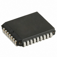
CY7B991V-7JC Cypress Semiconductor Corp, CY7B991V-7JC Datasheet - Page 9

CY7B991V-7JC
Manufacturer Part Number
CY7B991V-7JC
Description
IC CLK BUFF SKEW 8OUT 32PLCC
Manufacturer
Cypress Semiconductor Corp
Series
RoboClock™r
Type
Buffer/Driverr
Datasheet
1.CY7B991V-2JC.pdf
(13 pages)
Specifications of CY7B991V-7JC
Number Of Circuits
1
Ratio - Input:output
8:8
Differential - Input:output
Yes/Yes
Input
3-State
Output
LVTTL
Frequency - Max
80MHz
Voltage - Supply
2.97 V ~ 3.63 V
Operating Temperature
0°C ~ 70°C
Mounting Type
Surface Mount
Package / Case
32-PLCC
Frequency-max
80MHz
Lead Free Status / RoHS Status
Contains lead / RoHS non-compliant
Other names
428-1384
Available stocks
Company
Part Number
Manufacturer
Quantity
Price
Company:
Part Number:
CY7B991V-7JC
Manufacturer:
Cypress Semiconductor Corp
Quantity:
10 000
Part Number:
CY7B991V-7JC
Manufacturer:
CYPRESS/赛普拉斯
Quantity:
20 000
Company:
Part Number:
CY7B991V-7JCT
Manufacturer:
Cypress Semiconductor Corp
Quantity:
10 000
Operational Mode Descriptions
Figure 2 shows the LVPSCB configured as a zero-skew clock
buffer. In this mode the CY7B991V can be used as the basis
for a low-skew clock distribution tree. When all of the function
select inputs (xF0, xF1) are left open, the outputs are aligned
and may each drive a terminated transmission line to an inde-
pendent load. The FB input can be tied to any output in this
Figure 3 shows a configuration to equalize skew between met-
al traces of different lengths. In addition to low skew between
outputs, the LVPSCB can be programmed to stagger the tim-
ing of its outputs. The four groups of output pairs can each be
programmed to different output timing. Skew timing can be
adjusted over a wide range in small increments with the appro-
priate strapping of the function select pins. In this configuration
the 4Q0 output is fed back to FB and configured for zero skew.
The other three pairs of outputs are programmed to yield dif-
ferent skews relative to the feedback. By advancing the clock
signal on the longer traces or retarding the clock signal on
shorter traces, all loads can receive the clock pulse at the
same time.
Document #: 38-07141 Rev. **
SYSTEM
CLOCK
SYS-
TEM
CLOCK
FB
REF
FS
4F0
4F1
3F0
3F1
2F0
2F1
1F0
1F1
TEST
FB
REF
FS
4F0
4F1
3F0
3F1
2F0
2F1
1F0
1F1
TEST
LENGTH L1 = L2
Figure 2. Zero-Skew and/or Zero-Delay Clock Driver
LENGTH L1 = L2 = L3 = L4
4Q0
4Q1
3Q0
3Q1
2Q0
2Q1
1Q0
1Q1
Figure 3. Programmable-Skew Clock Driver
4Q0
4Q1
3Q0
3Q1
2Q0
2Q1
1Q0
1Q1
L3 < L2 by 6 inches
L4 > L2 by 6 inches
REF
REF
configuration and the operating frequency range is selected
with the FS pin. The low-skew specification, coupled with the
ability to drive terminated transmission lines (with impedances
as low as 50 ohms), allows efficient printed circuit board de-
sign.
In this illustration the FB input is connected to an output with
0-ns skew (xF1, xF0 = MID) selected. The internal PLL syn-
chronizes the FB and REF inputs and aligns their rising edges
to insure that all outputs have precise phase alignment.
Clock skews can be advanced by 6 time units (t
an output selected for zero skew as the feedback. A wider range of
delays is possible if the output connected to FB is also skewed.
Since “Zero Skew”, +t
groups, and since the PLL aligns the rising edges of REF and FB,
it is possible to create wider output skews by proper selection of the
xFn inputs. For example a +10 t
achieved by connecting 1Q0 to FB and setting 1F0 = 1F1 = GND,
3F0 = MID, and 3F1 = High. (Since FB aligns at –4 t
L1
L2
L3
L4
L1
L2
L3
L4
Z
Z
Z
0
Z
0
0
0
Z
Z
Z
0
0
Z
0
0
U
LOAD
LOAD
LOAD
LOAD
, and –t
7B991V–10
LOAD
LOAD
LOAD
LOAD
7B991V–9
U
U
between REF and 3Qx can be
are defined relative to output
3.3V RoboClock
CY7B991V
U
Page 9 of 13
) when using
U
and 3Qx


