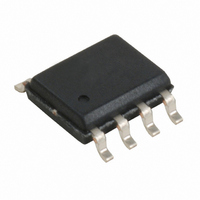
CY25814SXC Cypress Semiconductor Corp, CY25814SXC Datasheet - Page 4

CY25814SXC
Manufacturer Part Number
CY25814SXC
Description
IC CLOCK GEN 3.3V SS 8-SOIC
Manufacturer
Cypress Semiconductor Corp
Type
Clock/Frequency Synthesizer, Frequency Modulator, Spread Spectrum Clock Generatorr
Datasheet
1.CY25811SXC.pdf
(14 pages)
Specifications of CY25814SXC
Number Of Circuits
1
Package / Case
8-SOIC (3.9mm Width)
Pll
Yes
Input
Clock, Crystal, Resonator
Output
Clock
Ratio - Input:output
1:1
Differential - Input:output
No/No
Frequency - Max
128MHz
Divider/multiplier
Yes/Yes
Voltage - Supply
2.97 V ~ 3.63 V
Operating Temperature
0°C ~ 70°C
Mounting Type
Surface Mount
Frequency-max
128MHz
Maximum Input Frequency
32 MHz
Minimum Input Frequency
4 MHz
Output Frequency Range
16 MHz to 128 MHz
Supply Voltage (max)
3.63 V
Supply Voltage (min)
2.97 V
Maximum Operating Temperature
+ 70 C
Minimum Operating Temperature
0 C
Mounting Style
SMD/SMT
Operating Supply Voltage
3.3 V
Lead Free Status / RoHS Status
Lead free / RoHS Compliant
Lead Free Status / RoHS Status
Lead free / RoHS Compliant, Lead free / RoHS Compliant
Other names
428-2227-5
CY25814SXC
CY25814SXC
Available stocks
Company
Part Number
Manufacturer
Quantity
Price
Part Number:
CY25814SXC
Manufacturer:
CYPRESS/赛普拉斯
Quantity:
20 000
Company:
Part Number:
CY25814SXCT
Manufacturer:
CYPRESS
Quantity:
2 000
Spread Percentage Selection
The CY25811/12/14 SSCG products provide Center Spread, Down Spread, and No Spread functions. The amount of Spread
percentage is selected using 3-Level. S0 and S1 digital inputs and Spread percent values are given in
Table 3. Spread Percent Selection
3-Level Digital Inputs
S0, S1, and FRSEL digital inputs are designed to sense three
different logic levels designated as High “1”, Low “0”, and Middle
“M”. With this 3-Level digital input logic, the 3-Level Logic detects
nine different logic states.
S0, S1, and FRSEL pins include an on chip 20K (10K and 10K)
resistor divider. No external application resistors are needed to
implement the 3-level logic levels as shown here:
Logic Level “0”: 3–Level logic pin connected to GND.
Logic Level “M”: 3–Level logic pin left floating (no connection).
Logic Level “1”: 3–Level logic pin connected to V
Figure 2
Figure 2. 3–Level Logic
Document Number: 38-07112 Rev. *I
(MHz)
10-12
12-14
14-16
16-20
20-24
24-28
28-32
FRSEL
S0, S1
to VSS
8-10
XIN
4-5
5-6
6-7
7-8
and
LOW (0)
LOGIC
illustrates how to implement 3–Level Logic.
FRSEL
VSS
M
M
M
M
0
0
0
0
1
1
1
1
UNCONNECTED
Center
S1 = 0
S0 = 0
MIDDLE (M)
FRSEL
S0, S1
±1.4
±1.3
±1.2
±1.1
±1.4
±1.3
±1.2
±1.1
±1.4
±1.3
±1.2
±1.1
(%)
and
LOGIC
S0 = M
Center
S1 = 0
± 1.2
± 1.1
± 0.9
± 0.9
± 0.9
± 0.9
± 0.9
± 0.9
±1.2
±1.1
±1.2
±1.1
(%)
HIGH (H)
FRSEL
to VDD
S0, S1
LOGIC
Center
S1 = 0
S0 = 1
DD
and
± 0.6
± 0.5
± 0.5
± 0.4
± 0.6
± 0.5
± 0.5
± 0.4
± 0.6
± 0.5
± 0.5
± 0.4
(%)
.
S1 = M
Center
S0 = 0
± 0.5
± 0.4
± 0.4
± 0.3
± 0.5
± 0.4
± 0.4
± 0.3
± 0.5
± 0.4
± 0.4
± 0.3
(%)
Modulation Rate
SSCGs use frequency modulation (FM) to distribute energy over
a specific band of frequencies. The maximum frequency of the
clock (fmax) and minimum frequency of the clock (fmin)
determine this band of frequencies. The time required to
transition from fmin to fmax and back to fmin is the period of the
Modulation Rate. The Modulation Rate of SSCG clocks are
generally referred to in terms of frequency, or:
fmod = 1/Tmod.
The input clock frequency, fin, and the internal divider determine
the Modulation Rate.
In CY25811/2/4 devices, the (Spread Spectrum) modulation rate,
fmod, is given by the following formula:
fmod = fin/DR
Here fmod is the Modulation Rate, fin is the Input Frequency, and
DR is the Divider Ratio as given in
Frequency Range is set by FRSEL.
Table 4. Modulation Rate Divider Ratios
FRSEL
M
S1 = 1
S0 = 1
0
1
Down
–3.0
–2.7
–2.5
–2.3
–3.0
–2.7
–2.5
–2.3
–3.0
–2.7
–2.5
–2.3
(%)
Input Frequency Range
S1 = 1
S0 = 0
Down
–2.2
–1.9
–1.8
–1.7
–2.2
–1.9
–1.8
–1.7
–2.2
–1.9
–1.8
–1.7
(%)
16 to 32
8 to 16
(MHz)
4 to 8
S1 = M
S0 = 1
Down
–1.9
–1.7
–1.5
–1.4
–1.9
–1.7
–1.5
–1.4
–1.9
–1.7
–1.5
–1.4
(%)
Table
S0 = M
S1 = 1
Down
Table
CY25811/12/14
–0.7
–0.6
–0.6
–0.5
–0.7
–0.6
–0.6
–0.5
–0.7
–0.6
–0.6
–0.5
(%)
3.
4. Note that Input
Divider Ratio
No Spread
S1 = M
S0 = M
Page 4 of 14
(DR)
128
256
512
0
0
0
0
0
0
0
0
0
0
0
0
[+] Feedback


