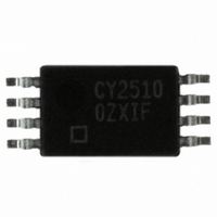
CY25100ZXIF Cypress Semiconductor Corp, CY25100ZXIF Datasheet - Page 6

CY25100ZXIF
Manufacturer Part Number
CY25100ZXIF
Description
IC CLOCK GEN PROG 8-TSSOP
Manufacturer
Cypress Semiconductor Corp
Type
Fanout Distribution, Spread Spectrum Clock Generatorr
Datasheet
1.CY25100SXCF.pdf
(14 pages)
Specifications of CY25100ZXIF
Number Of Circuits
1
Package / Case
8-TSSOP
Pll
Yes
Input
CMOS, Crystal
Output
CMOS
Ratio - Input:output
1:2
Differential - Input:output
No/No
Frequency - Max
200MHz
Divider/multiplier
Yes/No
Voltage - Supply
3.13 V ~ 3.45 V
Operating Temperature
-40°C ~ 85°C
Mounting Type
Surface Mount
Frequency-max
200MHz
Maximum Input Frequency
166 MHz
Minimum Input Frequency
8 MHz
Output Frequency Range
3 MHz to 200 MHz
Supply Voltage (max)
3.45 V
Supply Voltage (min)
3.13 V
Maximum Operating Temperature
+ 85 C
Minimum Operating Temperature
- 40 C
Mounting Style
SMD/SMT
Operating Supply Voltage
3.3 V
Lead Free Status / RoHS Status
Lead free / RoHS Compliant
For Use With
CY3690 - SOCKET ADAPTER FOR CY25100CY3691 - SOCKET ADAPTER FOR CY25100
Lead Free Status / Rohs Status
Lead free / RoHS Compliant
Other names
428-2221
CY25100ZXIF
CY25100ZXIF
Available stocks
Company
Part Number
Manufacturer
Quantity
Price
Company:
Part Number:
CY25100ZXIF
Manufacturer:
Cypress
Quantity:
827
Notes
Application Circuit
Switching Waveforms
Document #: 38-07499 Rev. *H
3. Because the load capacitors (C
4. If an external clock is used, apply the clock to XIN (pin 3) and leave XOUT (pin 2) floating (unconnected).
5. If SSON# (pin 8) is LOW (V
(Asynchronous)
capacitor (C
POWER
DOWN
CLKOUT
L
). Only a single 0.1-μF bypass capacitor is required on the V
V
0V
DD
SS
), the frequency modulation is on at SSCLK pin (pin 7).
XIN
and C
Refer to AC Electrical Characteristics table for SR (Slew Rate) values.
OUTPUT
Figure 4. Output Rise/Fall Time (SSCLK and REFCLK)
OUTPUT
XOUT
Figure 5. Power Down and Power Up Timing
) are provided by the CY25100, no external capacitors are needed on the XIN and XOUT pins to match the crystal load
P o w e r
Figure 3. Duty Cycle Timing (DC = t
t
STP
V
IL
Tr
Figure 2. Application Circuit Diagram
0 . 1 u F
High Impedance
V D D
Output Fall time (Tf) = (0.6 x V
Output Rise time (Tr) = (0.6 x V
1
2
3
4
V
P D # / O E
V D D
X I N / C L K I N
X O U T
t
IH
DD
1A
pin.
C Y 2 5 1 0 0
t
1B
DD
DD
Tf
)/SR2 (or SR4)
)/SR1 (or SR3)
R E F C L K
S S C L K
S S O N #
V S S
1A
/t
1B
8
7
6
5
[3, 4, 5]
)
t
PU
V
0V
DD
CY25100
Page 6 of 14
[+] Feedback


