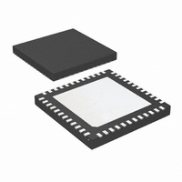
LMK04001BISQE/NOPB National Semiconductor, LMK04001BISQE/NOPB Datasheet - Page 42

LMK04001BISQE/NOPB
Manufacturer Part Number
LMK04001BISQE/NOPB
Description
IC CLOCK COND 1.5GHZ W/PLL 48LLP
Manufacturer
National Semiconductor
Series
PowerWise®r
Type
Clock Conditionerr
Datasheet
1.LMK04010BISQENOPB.pdf
(54 pages)
Specifications of LMK04001BISQE/NOPB
Pll
Yes
Input
LVCMOS
Output
LVCMOS, 2VPECL, LVPECL
Number Of Circuits
1
Ratio - Input:output
2:7
Differential - Input:output
Yes/Yes
Frequency - Max
1.57GHz
Divider/multiplier
Yes/Yes
Voltage - Supply
3.15 V ~ 3.45 V
Operating Temperature
-40°C ~ 85°C
Mounting Type
Surface Mount
Package / Case
48-LLP
Frequency-max
1.57GHz
Lead Free Status / RoHS Status
Lead free / RoHS Compliant
Other names
LMK04001BISQETR
Available stocks
Company
Part Number
Manufacturer
Quantity
Price
Company:
Part Number:
LMK04001BISQE/NOPB
Manufacturer:
NS
Quantity:
250
www.national.com
Note 45: Dynamic power dissipation of LVCMOS buffer varies with output frequency and can be found in the LVCMOS dynamic I
in Section 13.1 CLOCK OUTPUT AC CHARACTERISTICS. Total power dissipation of the LVCMOS buffer is the sum of static and dynamic power dissipation.
CLKoutXa and CLKoutXb are each considered an LVCMOS buffer.
Note 46: Assuming ThetaJ = 27.4 °C/W, the total power dissipated on chip must be less than 40/27.4 = 1450 mW to guarantee a junction temperature is less
than 125 °C.
Note 47: Worst case power dissipation can be estimated by multiplying typical power dissipation with a factor of 1.2.
Block
Entire device,
core current
REFMUX
LOS
Low Channel
Internal Buffer
High Channel
Internal Buffer
Divide circuitry
per output
Delay circuitry
per output
Fout Buffer
LVDS Buffer
LVPECL/
2VPECL Buffer
LVCMOS Buffer
(Note 45)
Entire device
(Single input
clock
(CLKIN_SEL = 0
or 1); LOS
disabled; PLL1
and PLL2 locked;
Fout disabled; All
CLKouts are on;
No delay); Divide
> 2 on each
output.
Condition
Single input clock (CLKIN_SEL = 0 or 1); LOS
disabled; PLL1 and PLL2 locked; All CLKouts are off;
No LVPECL emitter resistors connected
Enable auto-switch mode (CLKIN_SEL = 2 or 3)
Enable LOS (LOS_TYPE = 1, or 2, or 3)
The low channel internal buffer is enabled when
CLKout0 is enabled
The high channel internal buffer is enabled when one
of CLKout1 through CLKout4 is enabled
Divider bypassed (CLKout_MUX = 0, 2)
Divider enabled, divide = 2 (CLKout_MUX = 1, 3)
Divider enabled, divide > 2 (CLKout_MUX = 1, 3)
Delay bypassed (CLKout_MUX = 0, 1)
Delay enabled, delay < 8 (CLKout_MUX = 2, 3)
Delay enabled, delay > 7 (CLKout_MUX = 2, 3)
EN_Fout = 1
LVDS buffer, enabled
LVPECL/2VPECL buffer (enabled and with 120 Ω
emitter resistors)
LVPECL/2VPECL buffer (disabled and with 120 Ω
emitter resistors)
LVPECL/2VPECL (disabled and with no emitter
resistors)
LVCMOS buffer static I
LVCMOS buffer dynamic I
MHz
LMK0400x (Notes 46, 47)
LMK0401x (Notes 46, 47)
LMK0403x (Notes 46, 47)
TABLE 31. Typical Current Consumption for Selected Functional Blocks
CC
, C
CC
L
, C
= 5 pF
L
= 5 pF, CLKout = 100
42
(Temp = 25 °C,
V
Typical I
CC
379.5
377.5
337.1
(mA)
14.5
19.3
21.7
115
= 3.3 V)
4.3
3.6
5.3
8.5
5.8
9.9
4.5
10
10
40
16
0
0
0
CC
Dissipated in
device
Power
(mW)
1102
1012
380
996
14
12
33
33
17
28
19
33
48
64
82
47
15
53
0
0
0
CC
vs frequency plot, as shown
2VPECL Emitter
Dissipated in
Resistors
LVPECL/
Power
(mW)
150
250
100
50
25
-
-
-
-
-
-
-
-
-
-
-
-
-
-
-
-


