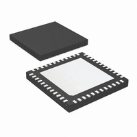
LMK04001BISQE/NOPB National Semiconductor, LMK04001BISQE/NOPB Datasheet - Page 9

LMK04001BISQE/NOPB
Manufacturer Part Number
LMK04001BISQE/NOPB
Description
IC CLOCK COND 1.5GHZ W/PLL 48LLP
Manufacturer
National Semiconductor
Series
PowerWise®r
Type
Clock Conditionerr
Datasheet
1.LMK04010BISQENOPB.pdf
(54 pages)
Specifications of LMK04001BISQE/NOPB
Pll
Yes
Input
LVCMOS
Output
LVCMOS, 2VPECL, LVPECL
Number Of Circuits
1
Ratio - Input:output
2:7
Differential - Input:output
Yes/Yes
Frequency - Max
1.57GHz
Divider/multiplier
Yes/Yes
Voltage - Supply
3.15 V ~ 3.45 V
Operating Temperature
-40°C ~ 85°C
Mounting Type
Surface Mount
Package / Case
48-LLP
Frequency-max
1.57GHz
Lead Free Status / RoHS Status
Lead free / RoHS Compliant
Other names
LMK04001BISQETR
Available stocks
Company
Part Number
Manufacturer
Quantity
Price
Company:
Part Number:
LMK04001BISQE/NOPB
Manufacturer:
NS
Quantity:
250
7.0 Absolute Maximum Ratings
If Military/Aerospace specified devices are required, please contact the National Semiconductor Sales Office/ Distributors
for availability and specifications.
Note 3: "Absolute Maximum Ratings" indicate limits beyond which damage to the device may occur. Operating Ratings indicate conditions for which the device
is intended to be functional, but do not guarantee specific performance limits. For guaranteed specifications and test conditions, see the Electrical Characteristics.
The guaranteed specifications apply only to the test conditions listed.
Note 4: This device is a high performance RF integrated circuit with an ESD rating up to 8 KV Human Body Model, up to 300 V Machine Model and up to 1,250
V Charged Device Model and is ESD sensitive. Handling and assembly of this device should only be done at ESD-free workstations.
Note 5: Stresses in excess of the absolute maximum ratings can cause permanent or latent damage to the device. These are absolute stress ratings only.
Functional operation of the device is only implied at these or any other conditions in excess of those given in the operation sections of the data sheet. Exposure
to absolute maximum ratings for extended periods can adversely affect device reliability.
Note 6: Never to exceed 3.6 V.
8.0 Package Thermal Resistance
Note 7: Specification assumes 16 thermal vias connect the die attach pad to the embedded copper plane on the 4-layer JEDEC board. These vias play a key
role in improving the thermal performance of the LLP. It is recommended that the maximum number of vias be used in the board layout.
9.0 Recommended Operating Conditions
Differential Input Current (CLKinX/X*, OSCin/
Supply Voltage
Temperature
Parameter
Ambient
Lead Temperature (solder 4 sec)
Storage Temperature Range
48-Lead LLP (Note 7)
Supply Voltage (Note 6)
Package
Input Voltage
Parameter
OSCin*)
Symbol
V
T
CC
A
V
Condition
CC
= 3.3 V
(Notes 3, 4, 5)
Symbol
T
V
V
T
I
STG
IN
CC
27.4° C/W
IN
L
3.15
Min
θ
-40
9
JA
Typical
-0.3 to (V
3.3
25
-0.3 to 3.6
-65 to 150
Ratings
+260
± 5
CC
+ 0.3)
θ
Max
3.45
J-PAD (Thermal Pad)
85
5.8° C/W
Units
mA
°C
°C
www.national.com
V
V
Unit
°C
V


