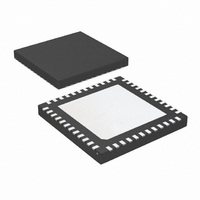
LMK04001BISQE/NOPB National Semiconductor, LMK04001BISQE/NOPB Datasheet - Page 47

LMK04001BISQE/NOPB
Manufacturer Part Number
LMK04001BISQE/NOPB
Description
IC CLOCK COND 1.5GHZ W/PLL 48LLP
Manufacturer
National Semiconductor
Series
PowerWise®r
Type
Clock Conditionerr
Datasheet
1.LMK04010BISQENOPB.pdf
(54 pages)
Specifications of LMK04001BISQE/NOPB
Pll
Yes
Input
LVCMOS
Output
LVCMOS, 2VPECL, LVPECL
Number Of Circuits
1
Ratio - Input:output
2:7
Differential - Input:output
Yes/Yes
Frequency - Max
1.57GHz
Divider/multiplier
Yes/Yes
Voltage - Supply
3.15 V ~ 3.45 V
Operating Temperature
-40°C ~ 85°C
Mounting Type
Surface Mount
Package / Case
48-LLP
Frequency-max
1.57GHz
Lead Free Status / RoHS Status
Lead free / RoHS Compliant
Other names
LMK04001BISQETR
Available stocks
Company
Part Number
Manufacturer
Quantity
Price
Company:
Part Number:
LMK04001BISQE/NOPB
Manufacturer:
NS
Quantity:
250
F
MHz. Using the data, this becomes:
In order to ensure startup of the oscillator circuit, the equiva-
lent series resistance (ESR) of the selected crystal should
conform to the specifications listed in the table of Electrical
Characteristics. It is also important to select a crystal with ad-
equate power dissipation capability, or drive level. If the drive
level supplied by the oscillator exceeds the maximum speci-
fied by the crystal manufacturer, the crystal will undergo
excessive aging and possibly become damaged. Drive level
is directly proportional to resonant frequency, capacitive load
seen by the crystal, voltage and equivalent series resistance
(ESR). For more complete coverage of crystal oscillator de-
sign,
www.national.com/analog/timing/clocking
www.national.com/appnotes.
17.8 TERMINATION AND USE OF CLOCK OUTPUT
(DRIVERS)
When terminating clock drivers keep in mind these guidelines
for optimum phase noise and jitter performance:
•
•
•
It is possible to drive a non-LVPECL or non-LVDS receiver
with an LVDS or LVPECL driver as long as the above guide-
lines are followed. Check the datasheet of the receiver or
input being driven to determine the best termination and cou-
pling method to be sure that the receiver is biased at its
optimum DC voltage (common mode voltage). For example,
when driving the OSCin/OSCin* input of the LMK04000 fam-
ily, OSCin/OSCin* should be AC coupled because OSCin/
OSCin* biases the signal to the proper DC level (See Figure
3) This is only slightly different from the AC coupled cases
described in Section 17.9.2 Driving CLKin Pins with a Single-
Ended Source because the DC blocking capacitors are
placed between the termination and the OSCin/OSCin* pins,
but the concept remains the same. The receiver (OSCin/OS-
Cin*) sets the input to the optimum DC bias voltage (common
mode voltage), not the driver.
17.8.1 Termination for DC Coupled Differential Operation
For DC coupled operation of an LVDS driver, terminate with
100 Ω as close as possible to the LVDS receiver as shown in
Figure 8.
NOM
Transmission line theory should be followed for good
impedance matching to prevent reflections.
Clock drivers should be presented with the proper loads.
For example:
— LVDS drivers are current drivers and require a closed
— LVPECL drivers are open emitters and require a DC
Receivers should be presented with a signal biased to
their specified DC bias level (common mode voltage) for
proper operation. Some receivers have self-biasing inputs
that automatically bias to the proper voltage level. In this
case, the signal should normally be AC coupled.
is the nominal frequency of the crystal and is in units of
current loop.
path to ground.
see
Application
Note
AN-1939
or
30027137
at
http://
http://
47
FIGURE 8. Differential LVDS Operation, DC Coupling, No
For DC coupled operation of an LVPECL driver, terminate
with 50 Ω to V
terminate with a Thevenin equivalent circuit (120 Ω resistor
connected to V
with the driver connected to the junction of the 120 Ω and 82
Ω resistors) as shown in Figure 10 for V
FIGURE 10. Differential LVPECL Operation, DC Coupling,
17.8.2 Termination for AC Coupled Differential Operation
AC coupling allows for shifting the DC bias level (common
mode voltage) when driving different receiver standards.
Since AC coupling prevents the driver from providing a DC
bias voltage at the receiver it is important to ensure the re-
ceiver is biased to its ideal DC level.
When driving non-biased LVDS receivers with an LVDS driv-
er, the signal may be AC coupled by adding DC blocking
capacitors, however the proper DC bias point needs to be
established at the receiver. One way to do this is with the ter-
mination circuitry in Figure 11.
FIGURE 9. Differential LVPECL Operation, DC Coupling
CC
CC
Biasing of the Receiver
and an 82 Ω resistor connected to ground
- 2 V as shown in Figure 9. Alternatively
Thevenin Equivalent
CC
= 3.3 V.
www.national.com
30027120
30027118
30027121


